JAJSKO0C October   2021  – November 2022 LMR51420

PRODUCTION DATA  

  1. 特長
  2. アプリケーション
  3. 概要
  4. Revision History
  5. Device Comparison Table
  6. Pin Configuration and Functions
  7. Specifications
    1. 7.1 Absolute Maximum Ratings
    2. 7.2 ESD Ratings
    3. 7.3 Recommended Operating Conditions
    4. 7.4 Thermal Information
    5. 7.5 Electrical Characteristics
    6. 7.6 System Characteristics
    7. 7.7 Typical Characteristics
  8. Detailed Description
    1. 8.1 Overview
    2. 8.2 Functional Block Diagram
    3. 8.3 Feature Description
      1. 8.3.1 Fixed Frequency Peak Current Mode Control
      2. 8.3.2 Adjustable Output Voltage
      3. 8.3.3 Enable
      4. 8.3.4 Minimum On Time, Minimum Off Time, and Frequency Foldback
      5. 8.3.5 Bootstrap Voltage
      6. 8.3.6 Overcurrent and Short-Circuit Protection
      7. 8.3.7 Soft Start
      8. 8.3.8 Thermal Shutdown
    4. 8.4 Device Functional Modes
      1. 8.4.1 Shutdown Mode
      2. 8.4.2 Active Mode
      3. 8.4.3 CCM Mode
      4. 8.4.4 Light-Load Operation (PFM Version)
      5. 8.4.5 Light-Load Operation (FPWM Version)
  9. Application and Implementation
    1. 9.1 Application Information
    2. 9.2 Typical Application
      1. 9.2.1 Design Requirements
      2. 9.2.2 Detailed Design Procedure
        1. 9.2.2.1 Custom Design With WEBENCH® Tools
        2. 9.2.2.2 Output Voltage Set-Point
        3. 9.2.2.3 Switching Frequency
        4. 9.2.2.4 Inductor Selection
        5. 9.2.2.5 Output Capacitor Selection
        6. 9.2.2.6 Input Capacitor Selection
        7. 9.2.2.7 Bootstrap Capacitor
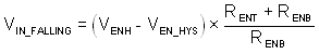
        8. 9.2.2.8 Undervoltage Lockout Set-Point
      3. 9.2.3 Application Curves
    3. 9.3 Power Supply Recommendations
    4. 9.4 Layout
      1. 9.4.1 Layout Guidelines
        1. 9.4.1.1 Compact Layout for EMI Reduction
        2. 9.4.1.2 Feedback Resistors
      2. 9.4.2 Layout Example
  10. 10Device and Documentation Support
    1. 10.1 Device Support
      1. 10.1.1 Third-Party Products Disclaimer
      2. 10.1.2 Development Support
        1. 10.1.2.1 Custom Design With WEBENCH® Tools
    2. 10.2 Documentation Support
      1. 10.2.1 Related Documentation
    3. 10.3 Receiving Notification of Documentation Updates
    4. 10.4 サポート・リソース
    5. 10.5 Trademarks
    6. 10.6 Electrostatic Discharge Caution
    7. 10.7 Glossary
  11. 11Mechanical, Packaging, and Orderable Information

パッケージ・オプション

メカニカル・データ(パッケージ|ピン)
サーマルパッド・メカニカル・データ
発注情報

Undervoltage Lockout Set-Point

The system undervoltage lockout (UVLO) is adjusted using the external voltage divider network of RENT and RENB. The UVLO has two thresholds, one for power up when the input voltage is rising and one for power down or brownouts when the input voltage is falling. Equation 15 can be used to determine the VIN UVLO level.

Equation 15. GUID-90765D6B-1EA5-494E-82F4-708089789FD2-low.gif

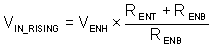
The EN rising threshold (VENH) for the LMR51420 is set to be 1.23 V (typical). Choose a value of 200 kΩ for RENB to minimize input current from the supply. If the desired VIN UVLO level is at 6.0 V, then the value of RENT can be calculated using Equation 16:

Equation 16. GUID-7A25E23E-CC63-44B2-82BD-B5AD2F3F7EAD-low.gif

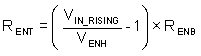
The above equation yields a value of 775.6 kΩ, a standard value of 768 kΩ is selected. The resulting falling UVLO threshold, equals 5.3 V, can be calculated by Equation 17 where EN hysteresis voltage, VEN_HYS, is 0.13 V (typical).

Equation 17. GUID-9F1D88E6-60AA-4143-9B23-ACB4DD3D946A-low.gif