JAJSAM4D September 2007 – August 2016 LMV641
PRODUCTION DATA.
- 1 特長
- 2 アプリケーション
- 3 概要
- 4 改訂履歴
- 5 Pin Configuration and Functions
- 6 Specifications
- 7 Detailed Description
- 8 Application and Implementation
- 9 Power Supply Recommendations
- 10Layout
- 11デバイスおよびドキュメントのサポート
- 12メカニカル、パッケージ、および注文情報
パッケージ・オプション
メカニカル・データ(パッケージ|ピン)
サーマルパッド・メカニカル・データ
発注情報
8 Application and Implementation
NOTE
Information in the following applications sections is not part of the TI component specification, and TI does not warrant its accuracy or completeness. TI’s customers are responsible for determining suitability of components for their purposes. Customers should validate and test their design implementation to confirm system functionality.
8.1 Application Information
The LMV641 is a low-power, low noise, wide-bandwidth operational amplifier with an extended power supply voltage range of 2.7 V to 12 V. With 10 MHz of gain bandwidth, 14 nV/√Hz input referred noise, and supply current of 138 μA, the LMV641 is well suited for portable applications that require precision while amplifying at high gains.
8.2 Typical Applications
8.2.1 High-Gain, Low-Power Inverting Amplifiers
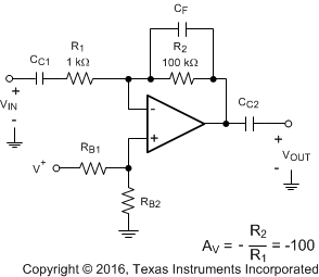 Figure 39. High-Gain Inverting Amplifier
8.2.1.1 Design Requirements
The wide unity-gain bandwidth allows these parts to provide large gain over a wide frequency range, while driving loads as low as 2 kΩ with less than 0.003% distortion.
8.2.1.2 Detailed Design Procedure
Figure 39 is an inverting amplifier, with a 100-kΩ feedback resistor, R2, and a 1-kΩ input resistor, R1, and provides a gain of −100. With the LMV641, these circuits can provide gain of −100 with a −3-dB bandwidth of 120 kHz, for a quiescent current as low as 116 µA. Coupling capacitors CC1 and CC2 can be added to isolate the circuit from DC voltages, while RB1 and RB2 provide DC biasing. A feedback capacitor CF can also be added to improve compensation.
8.2.1.3 Application Curve
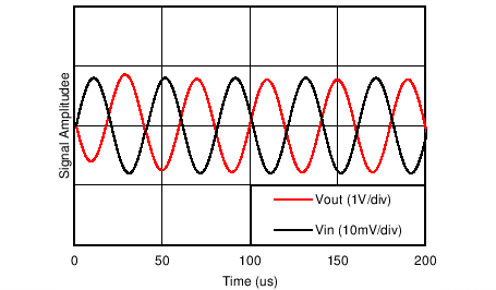 Figure 40. High Gain Inverting Amplifier Results
8.2.2 Anisotropic Magnetoresistive Sensor
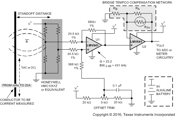 Figure 41. A Battery-Operated System for Contact-Less Current Sensing Using an Anisotropic Magnetoresistive Sensor
8.2.2.1 Design Requirements
The low operating current of the LMV641 makes it a good choice for battery-operated applications. Figure 41 shows two LMV641s in a portable application with a magnetic field sensor. The LMV641s condition the output from an anisotropic magnetoresistive (AMR) sensor. The sensor is arranged in the form of a Wheatstone bridge. This type of sensor can be used to accurately measure the current (either DC or AC) flowing in a wire by measuring the magnetic flux density, B, emanating from the wire.
8.2.2.2 Detailed Design Procedure
In this circuit, the use of a 9-V alkaline battery exploits the LMV641’s high voltage and low supply current for a low-power, portable-current-sensing application. The sensor converts an incident magnetic field (through the magnetic flux linkage) in the sensitive direction, to a balanced voltage output. The LMV641 can be used for moderate to high current sensing applications (from a few milliamps and up to 20 A) using a nearby external conductor providing the sensed magnetic field to the bridge. The circuit shows a Honeywell HMC1051Z used as a current sensor. Note that the circuit must be calibrated based on the final displacement of the sensed conductor relative to the measurement bridge. Typically, once the sensor has been oriented properly, with respect to the conductor to be measured, the conductor can be placed about one centimeter away from the bridge and have reasonable capability of measuring from tens of milliamperes to beyond 20 amperes.
In Figure 41, U1 is configured as a single differential input amplifier. Its input impedance is relatively low, however, and requires that the source impedance of the sensor be considered in the gain calculations. Also, the asymmetrical loading on the bridge will produce a small offset voltage that can be cancelled out with the offset trim circuit shown in Figure 41.
Figure 42 shows a typical magnetoresistive Wheatstone bridge and the Thevenin equivalent of its resistive elements. As we shall see, the Thevenin equivalent model of the sensor is useful in calculating the gain needed in the differential amplifier.
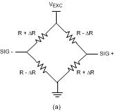
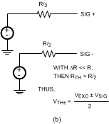 Figure 42. Anisotropic Magnetoresistive Wheatstone Bridge Sensor, (a),
and Thevenin Equivalent Circuit, (b)
Using Thevenin’s Theorem, the bridge can be reduced to two voltage sources with series resistances. ΔR is normally very small in comparison to R, thus the Thevenin equivalent resistance, commonly called the source resistance, can be taken to be R. When a bias voltage is applied between VEXC and ground, in the absence of a magnetic field, all of the resistances are considered equal. The voltage at Sig+ and Sig− is half VEXC, or 4.5 V, and Sig+ - Sig− = 0. Bridges are designed such that, when immersed in a magnetic field, opposite resistances in the bridge change by ±ΔR with an amount proportional to the strength of the magnetic field. This causes the bridge's output differential voltage, to change from its half VEXC value. Thus Sig+ - Sig− = Vsig ≠ 0. With four active elements, the output voltage is:

Because ΔR is proportional to the field strength, BS, the amount of output voltage from the sensor is a function of sensor sensitivity, S. This expression can rewritten as , where
where
- S = material constant (nominally 1 mV/V/gauss)
- BS = magnetic flux in gauss
A simplified schematic of a single op amp, differential amplifier is shown in Figure 43. The Thevenin equivalent circuit of the sensor can be used to calculate the gain of this amplifier.
 Figure 43. Differential Input Amplifier
The Honeywell HMC1051Z AMR sensor has nominal 1-kΩ elements and a sensitivity of 1 mV/V/gauss and is being used with 9 V of excitation with a full scale magnetic field range of ±6 gauss. At full-scale, the resistors will have ΔR ≈ 12 Ω and 108 mV will be seen from Sig− to Sig+ (see Figure 44).
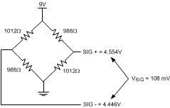 Figure 44. Sensor Output with No Load
Referring to the simplified diagram in Figure 43, and assuming that required full scale at the output of the amplifier is 2.5 V, a gain of 23.2 is needed for U1. It is clear from the Thevenin equivalent circuit in Figure 45 that a sensor Thevenin equivalent source resistance, RTHEV, of 500 Ω will be in series with both the inverting and noninverting inputs of the LMV641. Therefore, the required gain is:

Choosing R1 = R2 = 24.5 kΩ, then R4 will be approximately 580 kΩ. The actual values chosen will depend on the full-scale needs of the succeeding circuitry as well as bandwidth requirements. The values shown here provide a −3-dB bandwidth of approximately 431 kHz, and are found as follows.
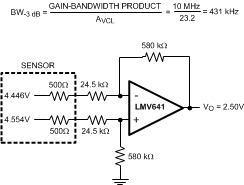 Figure 45. Thevenin Equivalent Showing Required Gain
By choosing input resistor values for R1 and R2 that are four to ten times the bridge element resistance, the bridge is minimally loaded and the offset errors induced by the op amp stages are minimized. These resistors should have 1% tolerance, or better, for the best noise rejection and offset minimization.
Referring once again to Figure 41, U2 is an additional gain stage with a thermistor element, RTH, in the feedback loop. It performs a temperature compensation function for the bridge so that it will have greater accuracy over a wide range of operational temperatures. With mangetoresistive sensors, temperature drift of the bridge sensitivity is negative and linear, and in the case of the sensor used here, is nominally −3000 PP/M. Thus the gain of U2 needs to increase proportionally with increasing temperature, suggesting a thermistor with a positive temperature coefficient. Selection of the temperature compensation resistor, RTH, depends on the additional gain required, on the thermistor chosen, and is dependent on the thermistor’s %/°C shift in resistance. For best op amp compatibility, the thermistor resistance should be greater than 1000 Ω. RTH should also be much less than RA, the feedback resistor. Because the temperature coefficient of the AMR bridge is largely linear, RTH also needs to behave in a linear fashion with temperature, thus RA is placed in parallel with RTH, which acts to linearize the thermistor.
8.2.2.2.1 Gain Error and Bandwidth Consideration if Using an Analog to Digital Converter
The bandwidth available from Figure 41 is dependent on the system closed loop gain required and the maximum gain-error allowed if driving an analog to digital converter (ADC). If the output from the sensor is intended to drive an ADC, the bandwidth will be considerably reduced from the closed-loop corner frequency. This is because the gain error of the pre-amplifier stage needs to be taken into account when calculating total error budget. Good practice dictates that the gain error of the amplifier be less than or equal to half LSB (preferably less in order to allow for other system errors that will eat up a portion of the available error budget) of the ADC. However, at the −3 dB corner frequency the gain error for any amplifier is 29.3%. In reality, the gain starts rolling off long before the −3 dB corner is reached. For example, if the amplifier is driving an 8-bit ADC, the minimum gain error allowed for half LSB would be approximately 0.2%. To achieve this gain error with the op amp, the maximum frequency of interest can be no higher than

where
- n is the bit resolution of the ADC
- f−3 dB is the closed loop corner frequency.
Given that the LMV641 has a GBW of 10 MHz, and is operating with a closed loop gain of 26.3, its closed loop bandwidth is 380 kHZ, therefore

which is the highest frequency that can be measured with required accuracy.
8.2.3 Voiceband Filter
The majority of the energy of recognizable speech is within a band of frequencies between 200 Hz and 4 kHz. Therefore, it is beneficial to design circuits which transmit telephone signals that pass only certain frequencies and eliminate unwanted signals (noise) that could interfere with conversations and introduce error into control signals. The pass band of these circuits is defined as the ranges of frequencies that are passed. A telephone system voice frequency (VF) channel has a pass band of 0 Hz to 4 kHz. Specifically for human voices most of the energy content is found from 300 Hz to 3 kHz and any signal within this range is considered an in-band signal. Alternatively, any signal outside this range but within the VF channel is considered an out-of-band signal.
To properly recover a voice signal in applications such as cellular phones, cordless phones, and voice pagers, a low power bandpass filter that is matched to the human voice spectrum can be implemented using an LMV641 op amp. Figure 46 shows a multi-feedback, multi-pole filter (2nd order response) with a gain of −1. The lower 3 dB cutoff frequency which is set by the DC blocking capacitor C1 and resistor R1 is 60 Hz and the upper cutoff frequency is 3.5 kHz.
The total current consumption is a mere 138 µA. The LV641 is operating with a gain of −1, but the circuit is easily modified to add gain. The op amp is powered from a single supply, hence the need for offset (common-mode) adjustment of its output, which is set to ½ VS via its non-inverting input.
This filter is also useful in applications for battery operated talking toys and games.
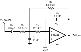 Figure 46. Low Power Voice In-Band Receive Filter for Battery-Powered Portable Use