SNOS534J February 2001 – November 2016 LMV712-N , LMV712-N-Q1
PRODUCTION DATA.
- 1 Features
- 2 Applications
- 3 Description
- 4 Revision History
- 5 Pin Configuration and Functions
- 6 Specifications
- 7 Detailed Description
- 8 Application and Implementation
- 9 Power Supply Recommendations
- 10Layout
- 11Device and Documentation Support
- 12Mechanical, Packaging, and Orderable Information
パッケージ・オプション
メカニカル・データ(パッケージ|ピン)
サーマルパッド・メカニカル・データ
発注情報
10 Layout
10.1 Layout Guidelines
To properly bypass the power supply, several locations on a printed circuit board must be considered. A 6.8 µF or greater tantalum capacitor must be placed at the point where the power supply for the amplifier is introduced onto the board. Another 0.1-µF ceramic capacitor must be placed as close as possible to the power supply pin of the amplifier. If the amplifier is operated in a single power supply, only the V+ pin requires bypassing with a 0.1-µF capacitor. If the amplifier is operated in a dual power supply, both V+ and V– pins must be bypassed.
It is good practice to use a ground plane on a printed circuit board to provide all components with a low inductive ground connection.
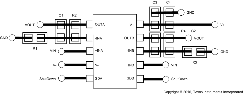
Surface mount components in 0805 size or smaller are recommended in the LMV712-N application circuits. Designers can take advantage of the DSBGA, WSON, and VSSOP miniature sizes to condense board layout to save space and reduce stray capacitance.
10.2 Layout Example
 Figure 38. Sample Layout of VSSOP