JAJSDJ1A June   2017  – January 2018 LMV722-Q1

PRODUCTION DATA.  

  1. 特長
  2. アプリケーション
  3. 概要
    1.     Device Images
      1.      概略回路図
  4. 改訂履歴
  5. Pin Configuration and Functions
    1.     Pin Functions
  6. Specifications
    1. 6.1 Absolute Maximum Ratings
    2. 6.2 ESD Ratings
    3. 6.3 Recommended Operating Conditions
    4. 6.4 Thermal Information
    5. 6.5 Electrical Characteristics VCC+ = 2.2 V
    6. 6.6 Electrical Characteristics VCC+ = 5 V
    7. 6.7 Typical Characteristics
  7. Detailed Description
    1. 7.1 Overview
    2. 7.2 Functional Block Diagram
    3. 7.3 Feature Description
      1. 7.3.1 Low Noise
      2. 7.3.2 Rail-to-Rail Output
      3. 7.3.3 Input Includes Ground
      4. 7.3.4 Signal Integrity
    4. 7.4 Device Functional Modes
  8. Application and Implementation
    1. 8.1 Application Information
    2. 8.2 Typical Application
      1. 8.2.1 Design Requirements
      2. 8.2.2 Detailed Design Procedure
      3. 8.2.3 Application Curve
  9. Power Supply Recommendations
    1. 9.1 Input and ESD Protection
  10. 10Layout
    1. 10.1 Layout Guidelines
    2. 10.2 Layout Example
  11. 11デバイスおよびドキュメントのサポート
    1. 11.1 ドキュメントのサポート
      1. 11.1.1 関連資料
    2. 11.2 ドキュメントの更新通知を受け取る方法
    3. 11.3 コミュニティ・リソース
    4. 11.4 商標
    5. 11.5 静電気放電に関する注意事項
    6. 11.6 Glossary
  12. 12メカニカル、パッケージ、および注文情報

パッケージ・オプション

メカニカル・データ(パッケージ|ピン)
サーマルパッド・メカニカル・データ
発注情報

Typical Characteristics

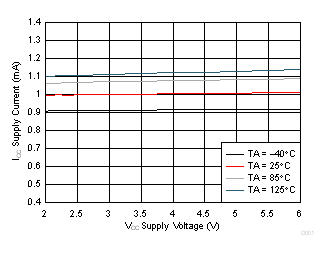
LMV722-Q1 D001_SLOS969.gif
Figure 1. Supply Current vs Supply Voltage
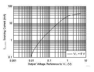
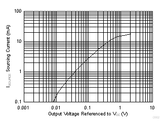
LMV722-Q1 D003_SLOS969.gif
Figure 3. Sourcing Current vs Output Voltage
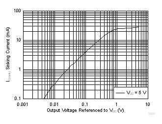
LMV722-Q1 D005_SLOS969.gif
Figure 5. Sinking Current vs Output Voltage
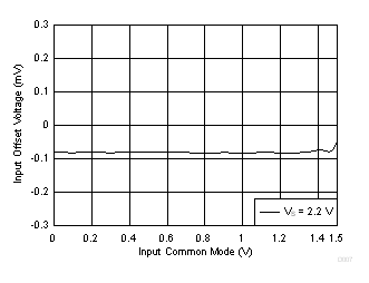
LMV722-Q1 D007_SLOS969.gif
Figure 7. Input Offset Voltage vs Input Common-Mode Voltage
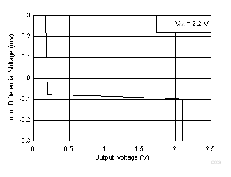
LMV722-Q1 D009_SLOS969.gif
Figure 9. Input Voltage vs Output Voltage
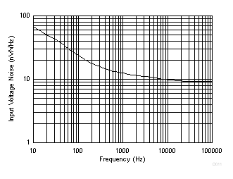
LMV722-Q1 D011_SLOS969.gif
Figure 11. Input Voltage Noise vs Frequency
LMV722-Q1 D013_SLOS969.gif
Figure 13. Psrr vs Frequency
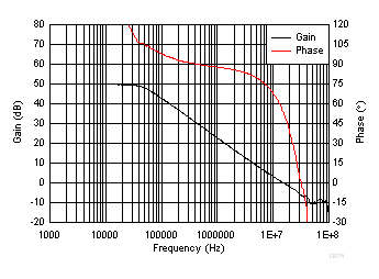
LMV722-Q1 D015_SLOS969.gif
VCC = 2.2 V
Figure 15. Gain And Phase vs Frequency
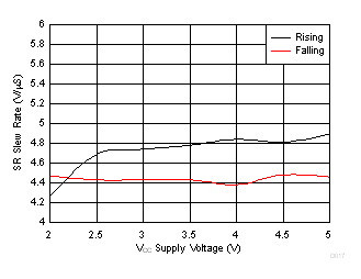
LMV722-Q1 D017_SLOS969.gif
Figure 17. Slew Rate vs Supply Voltage
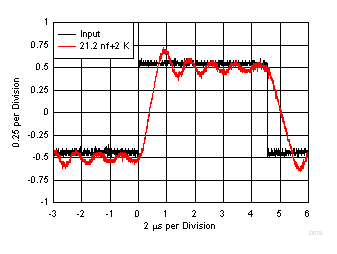
LMV722-Q1 D019_SLOS969.gif
VCC = 5 V, RL = 2 kΩ, CL = 21.2 nF, RO = 0 Ω
Figure 19. Pulse Response
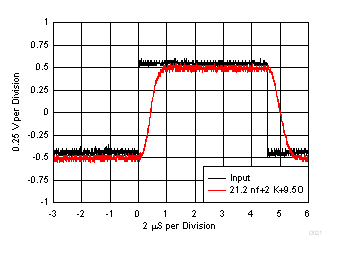
LMV722-Q1 D021_SLOS969.gif
VCC = 5 V, RL = 2 kΩ, CL = 21.2 nF, RO = 9.5 Ω
Figure 21. Pulse Response
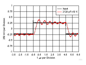
LMV722-Q1 D023_SLOS969.gif
VCC = 2.2 V, RL = 10 kΩ, CL = 2.12 nF, RO = 0 Ω
Figure 23. Pulse Response
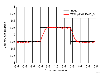
LMV722-Q1 D025_SLOS969.gif
VCC = 2.2 V, RL = 10 kΩ, CL = 2.12 nF, RO = 11.5 Ω
Figure 25. Pulse Response
LMV722-Q1 D002_SLOS969.gif
Figure 2. Sourcing Current vs Output Voltage
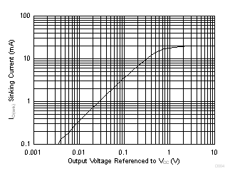
LMV722-Q1 D004_SLOS969.gif
VCC = 2.2 V
Figure 4. Sinking Current vs Output Voltage
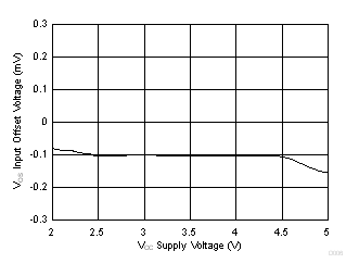
LMV722-Q1 D006_SLOS969.gif
Figure 6. VIO vs Supply Voltage
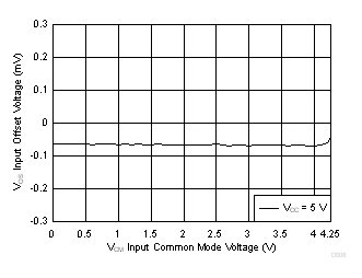
LMV722-Q1 D008_SLOS969.gif
Figure 8. Input Offset Voltage vs Input Common-Mode Voltage
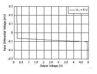
LMV722-Q1 D010_SLOS969.gif
Figure 10. Input Voltage vs Output Voltage
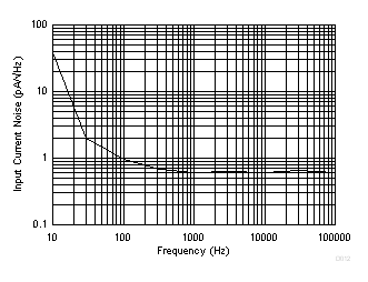
LMV722-Q1 D012_SLOS969.gif
Figure 12. Input Current Noise vs Frequency
LMV722-Q1 D014_SLOS969.gif
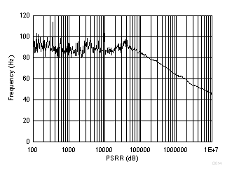
VCC = 5 V
Figure 14. Psrr vs Frequency
LMV722-Q1 D016_SLOS969.gif
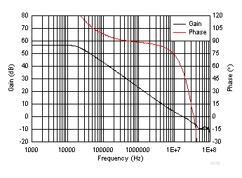
VCC = 5 V
Figure 16. Gain And Phase vs Frequency
LMV722-Q1 D018_SLOS969.gif
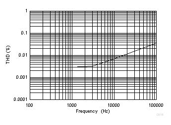
VCC = 2.2 V
Figure 18. Thd vs Frequency
LMV722-Q1 D020_SLOS969.gif
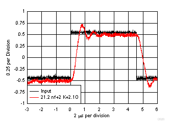
VCC = 5 V, RL = 2 kΩ, CL = 21.2 nF, RO = 2.1 Ω
Figure 20. Pulse Response
LMV722-Q1 D022_SLOS969.gif
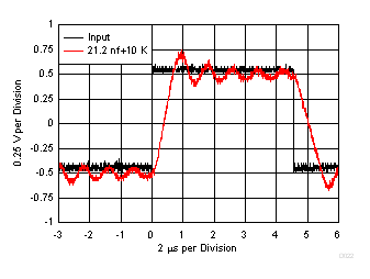
VCC = 5 V, RL = 10 kΩ, CL = 21.2 nF, RO = 0 Ω
Figure 22. Pulse Response
LMV722-Q1 D024_SLOS969.gif
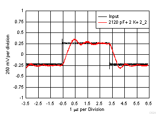
VCC = 2.2 V, RL = 10 kΩ, CL = 2.12 nF, RO = 2.2 Ω
Figure 24. Pulse Response