SNOS998I February 2002 – October 2015 LMV761 , LMV762 , LMV762Q-Q1
PRODUCTION DATA.
- 1 Features
- 2 Applications
- 3 Description
- 4 Revision History
- 5 Pin Configuration and Functions
-
6 Specifications
- 6.1 Absolute Maximum Ratings
- 6.2 ESD Ratings: LMV761, LMV762
- 6.3 ESD Ratings: LMV762Q-Q1
- 6.4 Recommended Operating Conditions
- 6.5 Thermal Information
- 6.6 2.7-V Electrical Characteristics
- 6.7 5-V Electrical Characteristics
- 6.8 2-V Switching Characteristics
- 6.9 5-V Switching Characteristics
- 6.10 Typical Characteristics
- 7 Detailed Description
- 8 Application and Implementation
- 9 Power Supply Recommendations
- 10Layout
- 11Device and Documentation Support
- 12Mechanical, Packaging, and Orderable Information
パッケージ・オプション
メカニカル・データ(パッケージ|ピン)
サーマルパッド・メカニカル・データ
発注情報
10 Layout
10.1 Layout Guidelines
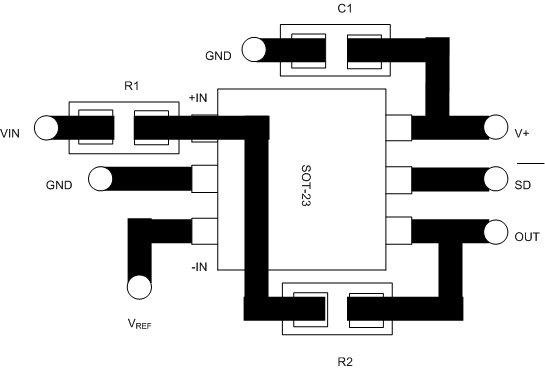
The LMV76x is designed to be stable and oscillation free, but it is still important to include the proper bypass capacitors and ground pick-ups. Ceramic 0.1-μF capacitors must be placed at both supplies to provide clean switching. Minimize the length of signal traces to reduce stray capacitance.
10.2 Layout Example
 Figure 26. Comparator With Hysteresis