JAJS595I August   1999  – June 2016 LMV821-N , LMV822-N , LMV822-N-Q1 , LMV824-N , LMV824-N-Q1

PRODUCTION DATA.  

  1. 特長
  2. アプリケーション
  3. 概要
  4. 改訂履歴
  5. Pin Configuration and Functions
  6. Specifications
    1. 6.1  Absolute Maximum Ratings
    2. 6.2  ESD Ratings
    3. 6.3  Recommended Operating Conditions
    4. 6.4  Thermal Information, 5 Pins
    5. 6.5  Thermal Information, 8 Pins
    6. 6.6  Thermal Information, 14 Pins
    7. 6.7  DC Electrical Characteristics 2.7V
    8. 6.8  DC Electrical Characteristics 2.5V
    9. 6.9  AC Electrical Characteristics 2.7V
    10. 6.10 DC Electrical Characteristics 5V
    11. 6.11 AC Electrical Characteristics 5V
    12. 6.12 Typical Characteristics
  7. Detailed Description
    1. 7.1 Overview
    2. 7.2 Functional Block Diagram
    3. 7.3 Feature Description
    4. 7.4 Device Functional Modes
      1. 7.4.1 Frequency and Phase Response Considerations
      2. 7.4.2 Unity Gain Pulse Response Consideration
      3. 7.4.3 Input Bias Current Consideration
  8. Application and Implementation
    1. 8.1 Application Information
    2. 8.2 Typical Applications
      1. 8.2.1 Telephone-Line Transceiver
        1. 8.2.1.1 Design Requirements
        2. 8.2.1.2 Detailed Design Procedure
      2. 8.2.2 “Simple” Mixer (Amplitude Modulator)
        1. 8.2.2.1 Design Requirements
        2. 8.2.2.2 Detailed Design Procedure
        3. 8.2.2.3 Application Performance Plot
      3. 8.2.3 Tri-Level Voltage Detector
        1. 8.2.3.1 Design Requirements
        2. 8.2.3.2 Detailed Design Procedure
        3. 8.2.3.3 Application Performance Plot
      4. 8.2.4 Dual Amplifier Active Filters (DAAFs)
        1. 8.2.4.1 Design Requirements
        2. 8.2.4.2 Detailed Design Procedure
        3. 8.2.4.3 Application Perfromance Plots
    3. 8.3 Do's and Don'ts
  9. Power Supply Recommendations
  10. 10Layout
    1. 10.1 Layout Guidelines
    2. 10.2 Layout Example
  11. 11デバイスおよびドキュメントのサポート
    1. 11.1 ドキュメントのサポート
      1. 11.1.1 関連資料
    2. 11.2 ドキュメントの更新通知を受け取る方法
    3. 11.3 コミュニティ・リソース
    4. 11.4 関連リンク
    5. 11.5 商標
    6. 11.6 静電気放電に関する注意事項
    7. 11.7 Glossary
  12. 12メカニカル、パッケージ、および注文情報

パッケージ・オプション

メカニカル・データ(パッケージ|ピン)
サーマルパッド・メカニカル・データ
発注情報

Layout

Layout Guidelines

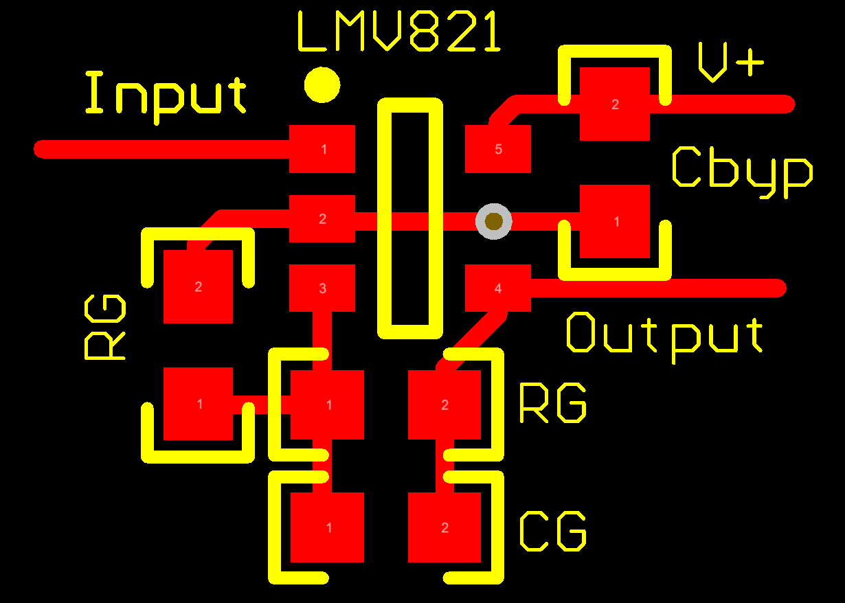
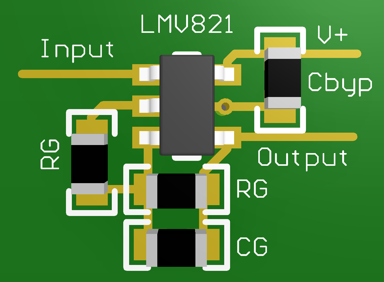
The V+ pin should be bypassed to ground with a low ESR capacitor.

The optimum placement is closest to the V+ and ground pins.

Care should be taken to minimize the loop area formed by the bypass capacitor connection between V+ and ground.

The ground pin should be connected to the PCB ground plane at the pin of the device.

The feedback components should be placed as close to the device as possible minimizing strays.

Layout Example

LMV821-N LMV822-N LMV822-N-Q1 LMV824-N LMV824-N-Q1 Layout.png Figure 47. 2-D Layout
LMV821-N LMV822-N LMV822-N-Q1 LMV824-N LMV824-N-Q1 3D-Layout.png Figure 48. 3-D Layout