JAJS972M November 2001 – September 2016 LMV981-N , LMV982-N
PRODUCTION DATA.
- 1 特長
- 2 アプリケーション
- 3 概要
- 4 改訂履歴
- 5 Description (continued)
- 6 Pin Configuration and Functions
-
7 Specifications
- 7.1 Absolute Maximum Ratings
- 7.2 ESD Ratings
- 7.3 Recommended Operating Conditions
- 7.4 Thermal Information
- 7.5 Electrical Characteristics - DC, 1.8 V
- 7.6 Electrical Characteristics - AC, 1.8 V
- 7.7 Electrical Characteristics - DC, 2.7 V
- 7.8 Electrical Characteristics - AC, 2.7 V
- 7.9 Electrical Characteristics - DC, 5 V
- 7.10 Electrical Characteristics - AC, 5 V
- 7.11 Typical Characteristics
- 8 Detailed Description
- 9 Application and Implementation
- 10Power Supply Recommendations
- 11Layout
- 12デバイスおよびドキュメントのサポート
- 13メカニカル、パッケージ、および注文情報
8 Detailed Description
8.1 Overview
The LMV98x-N are low-voltage, low-power operational amplifiers (op-amp) operating from 1.8-V to 5.5-V supply voltages and have rail-to-rail input and output with shutdown. LMV98x-N input common-mode voltage extends 200 mV beyond the supplies which enables user enhanced functionality beyond the supply voltage range.
8.2 Functional Block Diagram

8.3 Feature Description
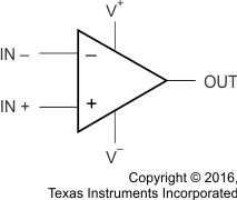
The differential inputs of the amplifier consist of a noninverting input (+IN) and an inverting input (–IN). The amplifer amplifies only the difference in voltage between the two inputs, which is called the differential input voltage. The output voltage of the op-amp VOUT is given by Equation 1:
where
- AOL is the open-loop gain of the amplifier, typically around 100 dB (100,000x, or 10 µV per volt).
8.4 Device Functional Modes
8.4.1 Input and Output Stage
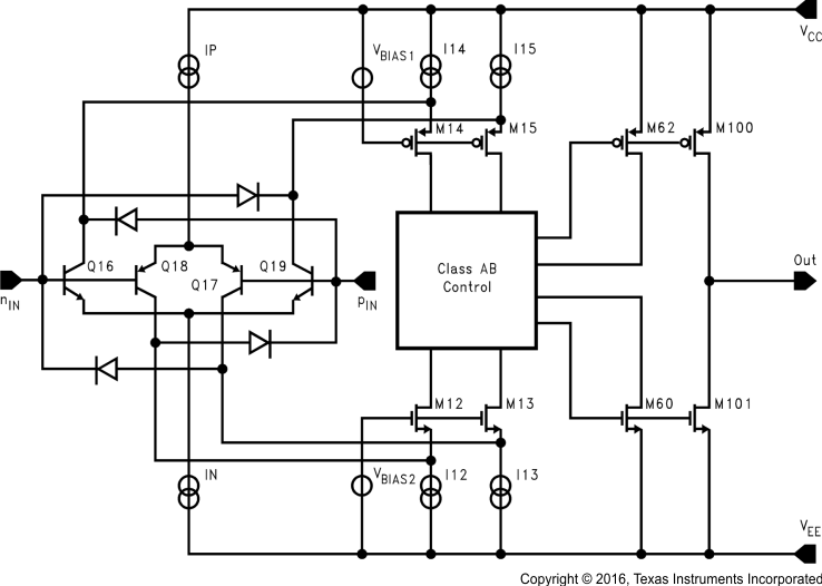
The rail-to-rail input stage of this family provides more flexibility for the designer. The LMV98x-N use a complimentary PNP and NPN input stage in which the PNP stage senses common-mode voltage near V− and the NPN stage senses common-mode voltage near V+. The transition from the PNP stage to NPN stage occurs
1 V below V+. Because both input stages have their own offset voltage, the offset of the amplifier becomes a function of the input common-mode voltage and has a crossover point at 1 V below V+.
 Figure 28. Simplified Schematic Diagram
This VOS crossover point can create problems for both DC− and AC-coupled signals if proper care is not taken. Large input signals that include the VOS crossover point causes distortion in the output signal. One way to avoid such distortion is to keep the signal away from the crossover. For example, in a unity gain buffer configuration with VS = 5 V, a 5-V peak-to-peak signal contains input-crossover distortion while a 3-V peak-to-peak signal centered at 1.5 V does not contain input-crossover distortion as it avoids the crossover point. Another way to avoid large signal distortion is to use a gain of −1 circuit which avoids any voltage excursions at the input terminals of the amplifier. In that circuit, the common-mode DC voltage can be set at a level away from the VOS cross-over point. For small signals, this transition in VOS shows up as a VCM dependent spurious signal in series with the input signal and can effectively degrade small-signal parameters such as gain and common-mode rejection ratio. To resolve this problem, the small signal must be placed such that it avoids the VOS crossover point. In addition to the rail-to-rail performance, the output stage can provide enough output current to drive
600-Ω loads. Because of the high-current capability, take care not to exceed the 150°C maximum junction temperature specification.
8.4.2 Shutdown Mode
The LMV98x-N family has a shutdown pin. To conserve battery life in portable applications, the LMV98x-N can be disabled when the shutdown pin voltage is pulled low. When in shutdown, the output stage is in a high-impedance state and the input bias current drops to less than 1 nA.
The shutdown pin cannot be left unconnected. In case shut-down operation is not required, the shutdown pin must be connected to V+ when the LMV98x-N are used. Leaving the shutdown pin floating results in an undefined operation mode, either shutdown or active, or even oscillating between the two modes.
8.4.3 Input Bias Current Consideration
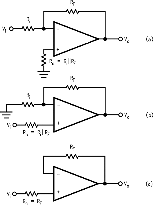
The LMV98x-N family has a complementary bipolar input stage. The typical input bias current (IB) is 15 nA. The input bias current can develop a significant offset voltage. This offset is primarily due to IB flowing through the negative feedback resistor, RF. For example, if IB is 50 nA and RF is 100 kΩ, then an offset voltage of 5 mV develops (VOS = IB x RF). Using a compensation resistor (RC), as shown in Figure 29, cancels this effect. But the input offset current (IOS) still contributes to an offset voltage in the same manner.
 Figure 29. Canceling the Offset Voltage due to Input Bias Current