SNAS187D February 2003 – January 2016 LMX2430 , LMX2433 , LMX2434
PRODUCTION DATA.
- 1 Features
- 2 Applications
- 3 Description
- 4 Revision History
- 5 Description continued
- 6 Pin Configuration and Functions
- 7 Specifications
- 8 Parameter Measurement Information
-
9 Detailed Description
- 9.1 Overview
- 9.2 Functional Block Diagram
- 9.3 Feature Description
- 9.4 Device Functional Modes
- 9.5 Programming
- 9.6
Register Maps
- 9.6.1 Control Register Content Map
- 9.6.2
R0 Register
- 9.6.2.1 RF_R[14:0] - RF Synthesizer Programmable Reference Divider (R Counter) (R0[17:3])
- 9.6.2.2 RF_CPP - RF Synthesizer Phase Detector Polarity (R0[18])
- 9.6.2.3 RF_CPG - RF Synthesizer Charge-Pump Current Gain (R0[19])
- 9.6.2.4 RF_CPT - RF Synthesizer Charge-Pump Tri-State (R0[20])
- 9.6.2.5 RF_RST - RF Synthesizer Counter Reset (R0[21])
- 9.6.3 R1 Register
- 9.6.4
R2 Register
- 9.6.4.1 RF_TOC[0:11] - RF Synthesizer Time-Out Counter (R2[14:3])
- 9.6.4.2
R3 Register
- 9.6.4.2.1 IF_R[14:0] - IF Synthesizer Programmable Reference Divider (R Counter) (R3[17:3])
- 9.6.4.2.2 IF_CPP - IF Synthesizer Phase Detector Polarity (R3[18])
- 9.6.4.2.3 IF_CPG - IF Synthesizer Charge-Pump Current Gain (R3[19])
- 9.6.4.2.4 IF_CPT - IF Synthesizer Charge-Pump Tri-State (R3[20])
- 9.6.4.2.5 IF_RST - IF Synthesizer Counter Reset (R3[21])
- 9.6.5 R4 Register
- 9.6.6 R5 Register
- 9.6.7 MUX[3:0] - Multifunction Output Select (R3[23:22]:R0[23:22])
- 10Application and Implementation
- 11Power Supply Recommendations
- 12Layout
- 13Device and Documentation Support
- 14Mechanical, Packaging, and Orderable Information
パッケージ・オプション
メカニカル・データ(パッケージ|ピン)
サーマルパッド・メカニカル・データ
発注情報
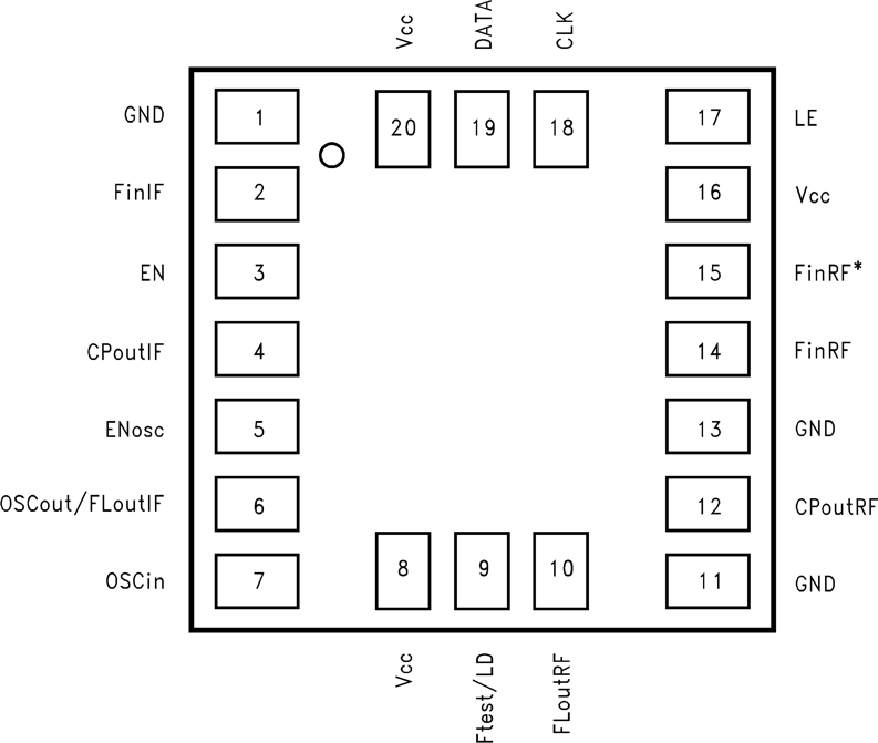
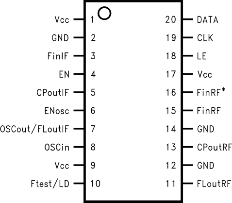
6 Pin Configuration and Functions
NPE Package
20-Pin ULGA Ultra Thin Chip Scale
Top View

PW Package
20-Pin TSSOP Thin Shrink Small Outline
Top View

Pin Functions
| PIN | I/O | DESCRIPTION | ||
|---|---|---|---|---|
| NAME | ULGA | TSSOP | ||
| CLK | 18 | 19 | I | MICROWIRE Clock input. High-impedance CMOS input. DATA is clocked into the 24-bit shift register on the rising edge of CLK. |
| CPoutIF | 4 | 5 | O | IF PLL charge-pump output. The output is connected to the external loop filter, which drives the input of the IF VCO. |
| CPoutRF | 12 | 13 | O | RF PLL charge-pump output. The output is connected to the external loop filter, which drives the input of the RF VCO. |
| DATA | 19 | 20 | I | MICROWIRE Data input. High-impedance CMOS input. Binary serial data. The MSB of DATA is shifted in first. The two last bits are the control bits. |
| EN | 3 | 4 | I | Chip Enable input. High-Impedance CMOS input. When this pin is set HIGH, the RF and IF PLLs are powered up. Power down is then controlled through the MICROWIRE. When this pin is set LOW, the device is asynchronously powered down, and the charge-pump output is forced to a high-impedance state (tri-state). |
| ENosc | 5 | 6 | I | Oscillator Enable input. High-impedance CMOS input. When this pin is set HIGH, the oscillator buffer is always powered up, independent of the state of the EN pin. When this pin is set LOW, the OSCout/ FLoutIF pin functions as an IF fastlock output, which connects a resistor in parallel to R2 of the external loop filter. |
| FinIF | 2 | 3 | I | IF PLL prescaler input. Small signal input from the VCO. |
| FLoutRF | 10 | 11 | O | RF PLL fastlock output. This pin connects a resistor in parallel to R2 of the external loop filter. This pin can also function as a general-purpose CMOS tri-state output. |
| FinRF | 14 | 15 | I | RF PLL prescaler input. Small-signal input from the VCO. |
| FinRF* | 15 | 16 | I | RF PLL prescaler complementary input. For single-ended operation, this pin must be AC grounded through a 100-pF capacitor. The LMX243x can be driven differentially when the AC-coupled capacitor is omitted. |
| Ftest/LD | 9 | 10 | O | Programmable multiplexed output. Functions as a general-purpose CMOS tri-state output, N and R divider output, RF/ IF PLL push-pull analog lock-detect output, RF/ IF PLL open-drain analog lock-detect output, or RF/ IF PLL digital filtered lock-detect output. |
| GND | 1 | 2 | — | Ground for the IF PLL analog and digital circuits, MICROWIRE, Ftest/LD and oscillator circuits. |
| 11 | 12 | |||
| 13 | 14 | |||
| LE | 17 | 18 | I | MICROWIRE Latch Enable input. High-impedance CMOS input. When LE transitions HIGH, DATA stored in the shift register is loaded into one of 6 internal control registers. |
| OSCout/ FLoutIF | 6 | 7 | O | Oscillator output/ IF PLL fastlock output. The output configuration is dependent on the state of the ENosc pin. When ENosc is set LOW, the pin functions as an IF fastlock output, which connects a resistor in parallel to R2 of the external loop filter. This configuration also functions as a general-purpose CMOS tri-state output. When ENosc is set HIGH, the pin functions as an oscillator output so that an external crystal can be used. |
| OSCin | 7 | 8 | I | Reference oscillator input. The input has an approximate Vcc/2 threshold and is driven by an external AC-coupled source. |
| Vcc | 16 | 17 | — | Power supply bias for the RF PLL analog circuits. Vcc may range from 2.25 V to 2.75 V. Bypass capacitors must be placed as close as possible to this pin and be connected directly to the ground plane. |
| 8 | 9 | |||
| 20 | 1 | |||