SNAS324B January   2006  – January 2016 LMX2486

PRODUCTION DATA.  

  1. Features
  2. Applications
  3. Description
  4. Revision History
  5. Pin Configuration and Functions
  6. Specifications
    1. 6.1 Absolute Maximum Ratings
    2. 6.2 ESD Ratings
    3. 6.3 Recommended Operating Conditions
    4. 6.4 Thermal Information
    5. 6.5 Electrical Characteristics
    6. 6.6 Timing Requirements
    7. 6.7 Typical Characteristics
      1. 6.7.1 Sensitivity
      2. 6.7.2 FinRF Input Impedance
      3. 6.7.3 FinIF Input Impedance
      4. 6.7.4 OSCin Input Impedance
      5. 6.7.5 Currents
  7. Parameter Measurements Information
    1. 7.1 Bench Test Set-Ups
      1. 7.1.1 Charge Pump Current Measurement
      2. 7.1.2 Charge Pump Current Specification Definitions
        1. 7.1.2.1 Charge Pump Output Current Variation vs Charge Pump Output Voltage
        2. 7.1.2.2 Charge Pump Output Current Variation vs Temperature
      3. 7.1.3 Sensitivity Measurement
      4. 7.1.4 Input Impedance Measurement
  8. Detailed Description
    1. 8.1 Overview
    2. 8.2 Functional Block Diagram
    3. 8.3 Feature Description
      1. 8.3.1 TCXO, Oscillator Buffer, and R Counter
      2. 8.3.2 Phase Detector
      3. 8.3.3 Charge Pump
      4. 8.3.4 Loop Filter
      5. 8.3.5 N Counters and High Frequency Input Pins
        1. 8.3.5.1 High Frequency Input Pins, FinRF and FinIF
        2. 8.3.5.2 Complementary High Frequency Pin, FinRF*
      6. 8.3.6 Digital Lock Detect Operation
      7. 8.3.7 Cycle Slip Reduction and Fastlock
        1. 8.3.7.1 Cycle Slip Reduction (CSR)
        2. 8.3.7.2 Fastlock
        3. 8.3.7.3 Using Cycle Slip Reduction (CSR) to Avoid Cycle Slipping
        4. 8.3.7.4 Using Fastlock to Improve Lock Times
        5. 8.3.7.5 Capacitor Dielectric Considerations for Lock Time
      8. 8.3.8 Fractional Spur and Phase Noise Controls
    4. 8.4 Device Functional Modes
      1. 8.4.1 Power Pins, Power-Down, and Power-Up Modes
    5. 8.5 Programming
      1. 8.5.1 General Programming Information
        1. 8.5.1.1 Register Location Truth Table
        2. 8.5.1.2 Control Register Content Map
    6. 8.6 Register Maps
      1. 8.6.1 R0 Register
        1. 8.6.1.1 RF_FN[11:0] -- Fractional Numerator for RF PLL
        2. 8.6.1.2 RF_N[10:0] -- RF N Counter Value
      2. 8.6.2 R1 Register
        1. 8.6.2.1 RF_FD[11:0] -- RF PLL Fractional Denominator
        2. 8.6.2.2 RF_R [5:0] -- RF R Divider Value
        3. 8.6.2.3 RF_P -- RF Prescaler bit
        4. 8.6.2.4 RF_PD -- RF Power Down Control Bit
      3. 8.6.3 R2 Register
        1. 8.6.3.1 IF_N[18:0] -- IF N Divider Value
        2. 8.6.3.2 IF_PD -- IF Power Down Bit
      4. 8.6.4 R3 Register
        1. 8.6.4.1 IF_R[11:0] -- IF R Divider Value
        2. 8.6.4.2 RF_CPG -- RF PLL Charge Pump Gain
        3. 8.6.4.3 Access -- Register Access Word
      5. 8.6.5 R4 Register
        1. 8.6.5.1 MUX[3:0] Frequency Out and Lock Detect MUX
        2. 8.6.5.2 IF_P -- IF Prescaler
        3. 8.6.5.3 RF_CPP -- RF PLL Charge Pump Polarity
        4. 8.6.5.4 IF_CPP -- IF PLL Charge Pump Polarity
        5. 8.6.5.5 OSC_OUT Oscillator Output Buffer Enable
        6. 8.6.5.6 OSC2X -- Oscillator Doubler Enable
        7. 8.6.5.7 FM[1:0] -- Fractional Mode
        8. 8.6.5.8 DITH[1:0] -- Dithering Control
        9. 8.6.5.9 ATPU -- PLL Automatic Power Up
      6. 8.6.6 R5 Register
        1. 8.6.6.1 Fractional Numerator Determination { RF_FN[21:12], RF_FN[11:0], Access[1] }
        2. 8.6.6.2 Fractional Denominator Determination { RF_FD[21:12], RF_FD[11:0], Access[1]}
      7. 8.6.7 R6 Register
        1. 8.6.7.1 RF_TOC -- RF Time-Out Counter and Control for FLoutRF Pin
        2. 8.6.7.2 RF_CPF -- RF PLL Fastlock Charge Pump Current
        3. 8.6.7.3 CSR[1:0] -- RF Cycle Slip Reduction
      8. 8.6.8 R7 Register
        1. 8.6.8.1 DIV4 -- RF Digital Lock Detect Divide By 4
        2. 8.6.8.2 IF_RST -- IF PLL Counter Reset
        3. 8.6.8.3 RF_RST -- RF PLL Counter Reset
        4. 8.6.8.4 RF_TRI -- RF Charge Pump TRI-STATE
        5. 8.6.8.5 IF_TRI -- IF Charge Pump TRI-STATE
  9. Application and Implementation
    1. 9.1 Application Information
    2. 9.2 Typical Application
      1. 9.2.1 Design Requirements
      2. 9.2.2 Detailed Design Procedure
      3. 9.2.3 Application Curves
  10. 10Power Supply Recommendations
  11. 11Layout
    1. 11.1 Layout Guidelines
    2. 11.2 Layout Example
  12. 12Device and Documentation Support
    1. 12.1 Community Resources
    2. 12.2 Trademarks
    3. 12.3 Electrostatic Discharge Caution
    4. 12.4 Glossary
  13. 13Mechanical, Packaging, and Orderable Information

パッケージ・オプション

メカニカル・データ(パッケージ|ピン)
サーマルパッド・メカニカル・データ
発注情報

9 Application and Implementation

NOTE

Information in the following applications sections is not part of the TI component specification, and TI does not warrant its accuracy or completeness. TI’s customers are responsible for determining suitability of components for their purposes. Customers should validate and test their design implementation to confirm system functionality.

9.1 Application Information

This device ideal for use in a broad class of applications, especially those requiring low current consumption and low fractional spurs. For applications that only need a single PLL, the unused PLL can be powered down and will not draw any extra current or generate any spurs or crosstalk.

9.2 Typical Application
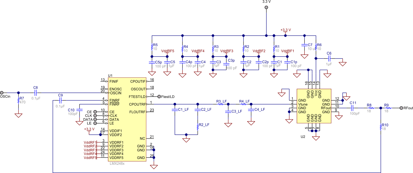
LMX2486 sch_apps_snas236.gif Figure 24. Typical Application

9.2.1 Design Requirements

Table 50 lists the design parameters of the LMX2486.

Table 50. Design Parameters

PARAMETER VALUE
PM Phase Margin 46.5 degrees
BW Loop Bandwidth 9.8 KHz
T3/T1 Pole Ratio 4.50%
T4/T3 57.70%
KPD Charge Pump Gain 8X (760 µA)
fPD Phase Detector Frequency 20 MHz
fVCO VCO Frequency 3200 – 3250
Vcc Supply 3 V
KVCO VCO Gain 90 MHz/V
CVCO VCO Input Capacitance 22 pF
C1_LF Loop Filter Components 6.8 nF
C2_LF 220 nF
C3_LF 4.7 nF
C4_LF 15 nF
R2_LF 150 Ω
R3_LF 56 Ω
R4_LF 33 Ω

9.2.2 Detailed Design Procedure

The design of the loop filter involves balancing requirements of lock time, spurs, and phase noise. This design is fairly involved, but the TI website has references, design tools, and simulation tools cover the loop filter design and simulation in depth.

9.2.3 Application Curves
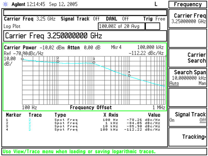
LMX2486 ta_phasenoise_snas324.gif Figure 25. Phase Noise
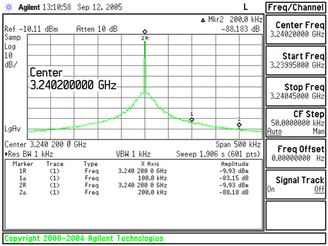
LMX2486 ta_spur_snas324.gif Figure 26. Fractional Spurs at 200-kHz Offset