SNOSCT6F March 2013 – January 2017 LP38798
PRODUCTION DATA.
- 1 Features
- 2 Applications
- 3 Description
- 4 Revision History
- 5 Pin Configuration and Functions
- 6 Specifications
- 7 Detailed Description
- 8 Application and Implementation
- 9 Power Supply Recommendations
- 10Layout
- 11Device and Documentation Support
- 12Mechanical, Packaging, and Orderable Information
6 Specifications
6.1 Absolute Maximum Ratings
over operating free-air temperature range (unless otherwise noted)(1)| MIN | MAX | UNIT | |
|---|---|---|---|
| VIN, VIN(CP) | –0.3 | 22 | V |
| VOUT, VOUT(FB) | –0.3 | VIN + 0.3 | V |
| VSET | –0.3 | VIN + 0.3 | V |
| VFB | –0.3 | VIN + 0.3 | V |
| VEN | –0.3 | 6 | V |
| Power dissipation(2) | Internally Limited | ||
| IOUT (Survival) | Internally Limited | ||
| Storage temperature, Tstg | –65 | 150 | °C |
(1) Stresses beyond those listed under Absolute Maximum Ratings may cause permanent damage to the device. These are stress ratings only, which do not imply functional operation of the device at these or any other conditions beyond those indicated under Recommended Operating Conditions. Exposure to absolute-maximum-rated conditions for extended periods may affect device reliability.
(2) The value of RθJA for the WSON package is dependent on PCB copper area, copper thickness, the number of copper layers in the PCB, and the number of thermal vias under the exposed thermal pad (DAP). Exceeding the maximum allowable power dissipation will cause excessive die temperature, and the regulator may go into thermal shutdown. See Thermal Considerations.
6.2 ESD Ratings
| VALUE | UNIT | |||
|---|---|---|---|---|
| V(ESD) | Electrostatic discharge | Human-body model (HBM), per ANSI/ESDA/JEDEC JS-001(1) | ±2000 | V |
| Charged-device model (CDM), per JEDEC specification JESD22-C101(2) | ±250 | |||
(1) JEDEC document JEP155 states that 500-V HBM allows safe manufacturing with a standard ESD control process.
6.3 Recommended Operating Conditions
| MIN | MAX | UNIT | |
|---|---|---|---|
| Input voltage, VIN | 3 | 20 | V |
| Output voltage, VOUT | 1.2 | (VIN – VDO) | V |
| Enable voltage, VEN | 0 | 5 | V |
| Junction temperature, TJ | –40 | 125 | °C |
6.4 Thermal Information
| THERMAL METRIC(1) | LP38798 | UNIT | |
|---|---|---|---|
| DNT (WSON) | |||
| 12 PINS | |||
| RθJA | Junction-to-ambient thermal resistance | 35.4 | °C/W |
| RθJC(top) | Junction-to-case (top) thermal resistance | 29.4 | °C/W |
| RθJB | Junction-to-board thermal resistance | 12.6 | °C/W |
| ψJT | Junction-to-top characterization parameter | 0.2 | °C/W |
| ψJB | Junction-to-board characterization parameter | 12.8 | °C/W |
| RθJC(bot) | Junction-to-case (bottom) thermal resistance | 2.6 | °C/W |
(1) For more information about traditional and new thermal metrics, see Semiconductor and IC Package Thermal Metrics.
6.5 Electrical Characteristics
Unless otherwise stated the following conditions apply: VIN = 5.5 V, VSET = 5 V, CCP = 10 nF X7R, CIN = 10 μF, 50-mΩ tantalum, COUT = 10 μF X7R MLCC, IOUT = 10 mA, and TJ = –40°C to +125°C.| PARAMETER | TEST CONDITIONS | MIN(1) | TYP(2) | MAX(1) | UNIT | |
|---|---|---|---|---|---|---|
| VFB | Feedback voltage | VIN = 5.5 V TJ = 25°C |
1.188 | 1.2 | 1.212 | V |
| 5.5 V ≤ VIN ≤ 20 V | 1.176 | 1.2 | 1.224 | |||
| VOS | VOUT – VSET | 0 | 3.5 | 16 | mV | |
| IFB | Feedback pin current | VFB = 1.2 V | 0 | 1 | µA | |
| ISET | SET pin internal current sink | VIN = 3 V, VSET = 2.5 V | 46 | μA | ||
| VIN = 5.5 V, VSET = 5 V | 25.2 | 52 | 67.8 | |||
| VIN = 12.5 V, VSET = 12 V | 71 | |||||
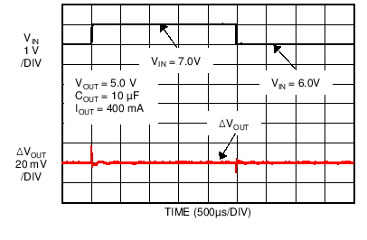
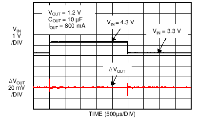
| ΔVOUT / ΔVIN | Line regulation(3) | 5.5 V ≤ VIN ≤ 20 V IOUT = 10 mA |
0.005 | %/V | ||
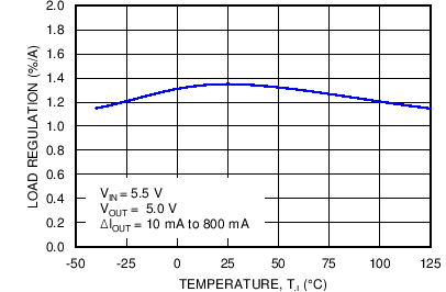
| ΔVOUT / ΔIOUT | Load regulation(4) | VIN = 5.5 V 10 mA ≤ IOUT ≤ 800 mA |
–0.2 | %/A | ||
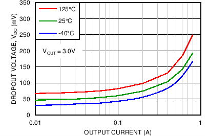
| VDO | Dropout voltage(5) | IOUT = 800 mA | 200 | 420 | mV | |
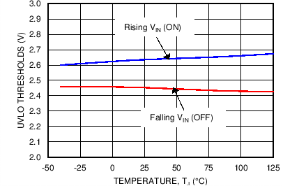
| UVLO | Undervoltage lock-out | VIN Rising until output is On | 2.47 | 2.65 | 2.83 | V |
| ΔUVLO | UVLO hysteresis | VIN Falling from > UVLO threshold until output is Off | 180 | mV | ||
| IGND | Ground pin current(6) | IOUT = 800 mA | 1.4 | 2.25 | mA | |
| VIN = 20 V, IOUT = 800 mA | 1.6 | 2.51 | ||||
| IQ | Ground pin current, quiescent(6) | IOUT = 0 mA | 1.4 | 2.1 | mA | |
| VIN = 20 V, IOUT = 0 mA | 1.5 | 2.2 | ||||
| ISD | Ground pin current, shutdown(6) | VEN = 0 V | 9 | 20 | µA | |
| VIN = 20 V, VEN = 0 V | 12 | 40 | ||||
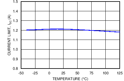
| ISC | Short-circuit current | RLOAD = 0 Ω | 850 | 1200 | 1600 | mA |
| ΔVCP | VCP – VIN | 2.8 | V | |||
| VIN = 20 V | 2.3 | |||||
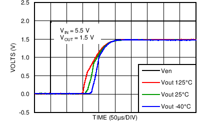
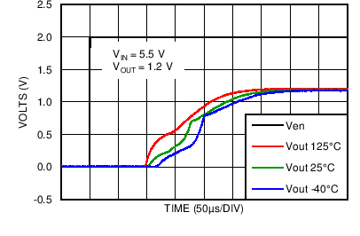
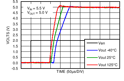
| tSTART | Start-up time | From VEN > VEN(ON) to VOUT ≥ 98% of VOUT(NOM) | 155 | 300 | µs | |
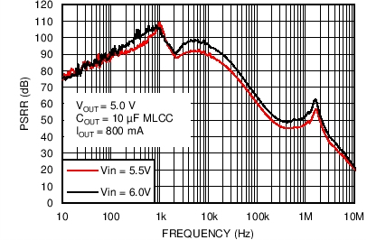
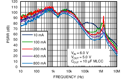
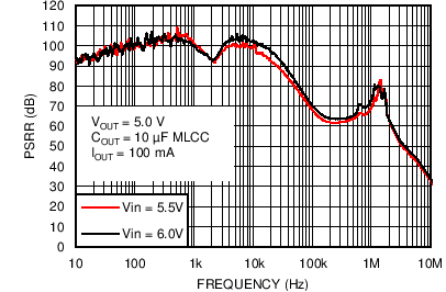
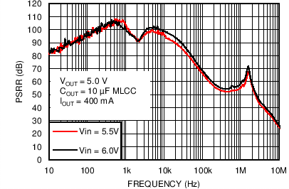
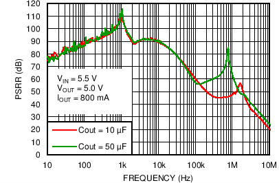
| PSRR | Power Supply Rejection Ratio | VOUT = 1.2 V, f = 10 kHz | 110 | dB | ||
| VOUT = 5 V, f = 10 kHz | 90 | |||||
| VOUT = 1.2 V, f = 100 kHz | 90 | |||||
| VOUT = 5 V, f = 100 kHz | 60 | |||||
| VOUT = 1.2 V, f = 1 MHz | 70 | |||||
| VOUT = 5 V, f = 1 MHz | 60 | |||||
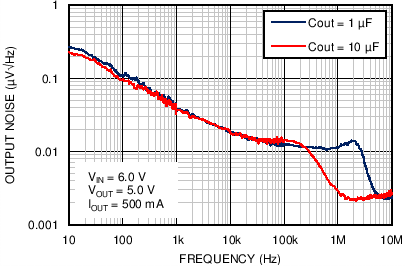
| eN | Output noise voltage (RMS) | VIN = 3 V, VOUT = 1.2 V COUT = 1 µF X7R BW = 10 Hz to 100 kHz |
4.96 | µV(RMS) | ||
| VIN = 3 V, VOUT = 1.2 V BW = 10 Hz to 100 kHz |
5.21 | |||||
| VIN = 3 V, VOUT = 1.2 V BW = 10 Hz to 10 MHz |
11.53 | |||||
| VIN = 6 V, VOUT = 5 V COUT = 1 µF X7R BW = 10 Hz to 100 kHz |
5.38 | |||||
| VIN = 6 V, VOUT = 5 V BW = 10 Hz to 100 kHz |
5.43 | |||||
| VIN = 6 V, VOUT = 5 V BW = 10 Hz to 10 MHz |
11.58 | |||||
| ENABLE INPUT | ||||||
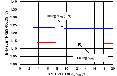
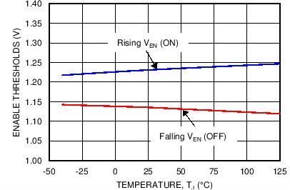
| VEN(ON) | Enable ON threshold voltage | VEN rising from 500 mV until Output is ON | 1.14 | 1.24 | 1.34 | V |
| ΔVEN | Enable threshold voltage hysteresis | VEN falling from VEN(ON) | 110 | mV | ||
| IEN(IL) | EN pin pullup current | VEN = 500 mV | 2 | 3 | µA | |
| IEN(IH) | EN pin pullup current | VEN = 2 V | 2 | 3 | ||
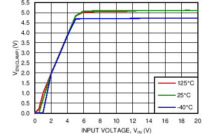
| VEN(CLAMP) | Enable pin clamp voltage | EN pin = Open | 5 | V | ||
| THERMAL SHUTDOWN | ||||||
| TSD | Thermal shutdown | Junction temperature (TJ) rising | 170 | °C | ||
| ΔTSD | Thermal shutdown hysteresis | Junction temperature (TJ) falling from TSD | 12 | |||
(1) Minimum and maximum limits are ensured through test, design, or statistical correlation over the operating junction temperature (TJ ) range of –40°C to 125°C, unless otherwise stated.
(2) Typical values represent the most likely parametric norm at TJ = 25°C, and are provided for reference purposes only.
(3) Line Regulation: % change in VOUT(NOM) for every 1V change in VIN= (( ΔVOUT / VOUT(NOM)) / ΔVIN ) × 100%
(4) Load Regulation: % change in VOUT(NOM) for every 1A change in IOUT = (( ΔVOUT / VOUT(NOM) ) / ΔIOUT ) × 100%
(5) Dropout voltage (VDO) is defined as the differential voltage measured between VOUT and VIN when VIN, falling from VIN = VOUT + 1 V, causes VOUT to drop 2% below the value measured with VIN = VOUT + 1 V. Dropout voltage specification does not apply when the programmed output voltage is below the Minimum Operating Input Voltage.
(6) Ground pin current is the sum of the current in both GND pins (pin 4 and pin 5) only, and does not include current from the SET pin.
6.6 Typical Characteristics
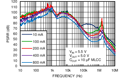
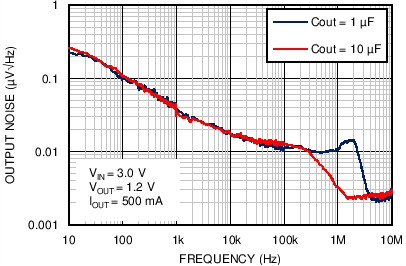
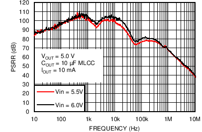
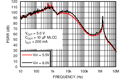
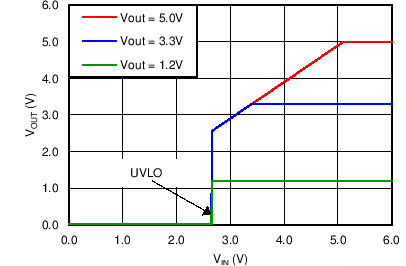
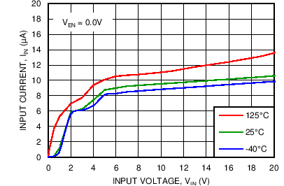
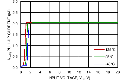
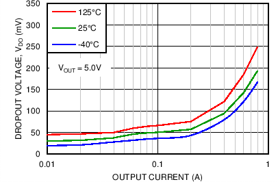
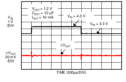
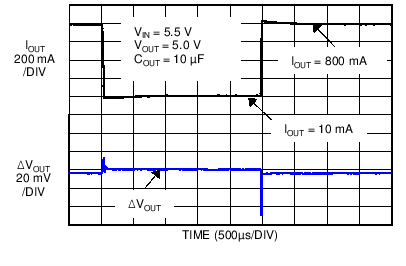
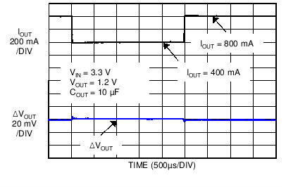
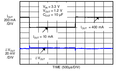
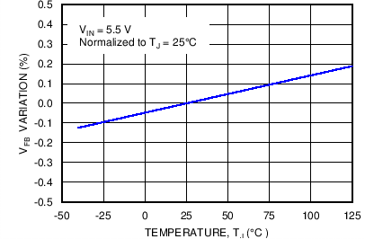
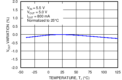
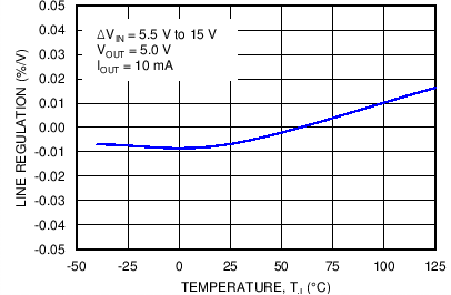
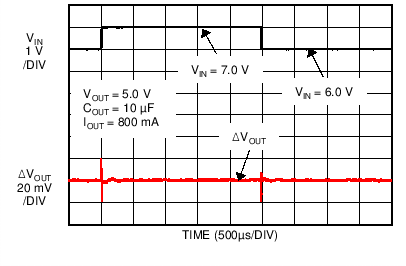
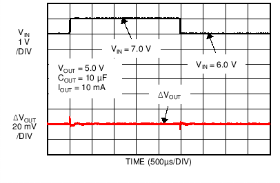
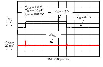
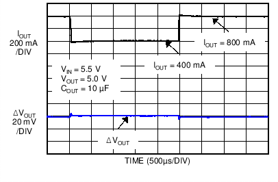
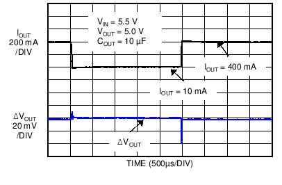
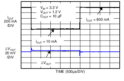
Unless otherwise specified: VIN = 5.5 V, VOUT = 5 V, IOUT = 10 mA, COUT = 10 µF MLCC 16 V X7R, and TJ = 25°C.