SNVS251J May 2004 – September 2014 LP3990
PRODUCTION DATA.
- 1 Features
- 2 Applications
- 3 Description
- 4 Revision History
- 5 Pin Configuration and Functions
- 6 Specifications
- 7 Detailed Description
- 8 Application and Implementation
- 9 Power Supply Recommendations
- 10Layout
- 11Device and Documentation Support
- 12Mechanical, Packaging, and Orderable Information
パッケージ・オプション
メカニカル・データ(パッケージ|ピン)
サーマルパッド・メカニカル・データ
発注情報
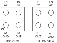
5 Pin Configuration and Functions
DSBGA (YZR)
4 Pins
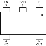
SOT-23 (DBV)
5 Pins
WSON (NGG)
6 Pins
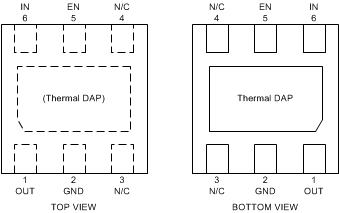
Pin Functions
| PIN | I/O | DESCRIPTION | |||
|---|---|---|---|---|---|
| NAME | DSBGA | SOT-23 | WSON | ||
| YZR | DBV | NGG | |||
| GND | A1 | 2 | 2 | — | Common Ground. |
| EN | A2 | 3 | 5 | I | Enable Input; Enables the Regulator when ≥ 0.95 V. Disables the Regulator when ≤ 0.4 V. Enable Input has 1-MΩ (typical) pull-down resistor to GND. |
| OUT | B1 | 5 | 1 | O | Voltage output. A 1-µF Low ESR Capacitor should be connected to this Pin. Connect this output to the load circuit. |
| IN | B2 | 1 | 6 | I | Voltage supply Input. A 1-µF capacitor should be connected at this input. |
| N/A | 4 | 3 | I | No internal connection. | |
| N/C | N/A | 4 | I | No internal connection. | |
| N/C | Pad | — | Thermal pad. Connect to Pin 2. | ||