JAJSLM6 March   2021 LP87702

PRODUCTION DATA  

  1. 特長
  2. アプリケーション
  3. 概要
  4. Revision History
  5. Pin Configuration and Functions
  6. Specifications
    1. 6.1 Absolute Maximum Ratings
    2. 6.2 ESD Ratings
    3. 6.3 Recommended Operating Conditions
    4. 6.4 Thermal Information
    5. 6.5 Electrical Characteristics
    6. 6.6 I2C Serial Bus Timing Parameters
    7. 6.7 Typical Characteristics
  7. Detailed Description
    1. 7.1 Overview
    2. 7.2 Functional Block Diagram
    3. 7.3 Feature Descriptions
      1. 7.3.1  Step-Down DC/DC Converters
        1. 7.3.1.1 Overview
        2. 7.3.1.2 Transition Between PWM and PFM Modes
        3. 7.3.1.3 Buck Converter Load Current Measurement
      2. 7.3.2  Boost Converter
      3. 7.3.3  Spread-Spectrum Mode
      4. 7.3.4  Sync Clock Functionality
      5. 7.3.5  Power-Up
      6. 7.3.6  Buck and Boost Control
        1. 7.3.6.1 Enabling and Disabling Converters
        2. 7.3.6.2 Changing Buck Output Voltage
      7. 7.3.7  Enable and Disable Sequences
      8. 7.3.8  Window Watchdog
      9. 7.3.9  Device Reset Scenarios
      10. 7.3.10 Diagnostics and Protection Features
        1. 7.3.10.1 Voltage Monitorings
        2. 7.3.10.2 Interrupts
        3. 7.3.10.3 Power-Good Information to Interrupt, PG0, and PG1 Pins
          1. 7.3.10.3.1 PGx Pin Gated (Unusual) Mode
          2. 7.3.10.3.2 PGx Pin Operation in Continuous Mode
          3. 7.3.10.3.3 Summary of PG0, PG1 Gated, and Continuous Operating Modes
        4. 7.3.10.4 Warning Interrupts for System Level Diagnostics
          1. 7.3.10.4.1 Output Power Limit
          2. 7.3.10.4.2 Thermal Warning
        5. 7.3.10.5 Protections Causing Converter Disable
          1. 7.3.10.5.1 Short-Circuit and Overload Protection
          2. 7.3.10.5.2 Overvoltage Protection
          3. 7.3.10.5.3 Thermal Shutdown
        6. 7.3.10.6 Protections Causing Device Power Down
          1. 7.3.10.6.1 Undervoltage Lockout
      11. 7.3.11 OTP Error Correction
      12. 7.3.12 Operation of GPO Signals
      13. 7.3.13 Digital Signal Filtering
    4. 7.4 Device Functional Modes
      1. 7.4.1 Modes of Operation
    5. 7.5 Programming
      1. 7.5.1 I2C-Compatible Interface
        1. 7.5.1.1 Data Validity
        2. 7.5.1.2 Start and Stop Conditions
        3. 7.5.1.3 Transferring Data
        4. 7.5.1.4 I2C-Compatible Chip Address
        5. 7.5.1.5 Auto Increment Feature
    6. 7.6 Register Maps
      1. 7.6.1 Register Descriptions
        1. 7.6.1.1 LP8770_map Registers
  8. Application and Implementation
    1. 8.1 Application Information
    2. 8.2 Typical Application
      1. 8.2.1 Design Requirements
      2. 8.2.2 Detailed Design Procedure
        1. 8.2.2.1 Application Components
          1. 8.2.2.1.1 Inductor Selection
          2. 8.2.2.1.2 Buck Input Capacitor Selection
          3. 8.2.2.1.3 Buck Output Capacitor Selection
          4. 8.2.2.1.4 Boost Input Capacitor Selection
          5. 8.2.2.1.5 Boost Output Capacitor Selection
          6. 8.2.2.1.6 Supply Filtering Components
      3. 8.2.3 Current Limit vs Maximum Output Current
      4. 8.2.4 Application Curves
  9. Power Supply Recommendations
  10. 10Layout
    1. 10.1 Layout Guidelines
    2. 10.2 Layout Example
  11. 11Device and Documentation Support
    1. 11.1 Third-Party Products Disclaimer
    2. 11.2 Receiving Notification of Documentation Updates
    3. 11.3 サポート・リソース
    4. 11.4 Trademarks
    5. 11.5 静電気放電に関する注意事項
    6. 11.6 用語集
  12. 12Mechanical, Packaging, and Orderable Information

パッケージ・オプション

メカニカル・データ(パッケージ|ピン)
サーマルパッド・メカニカル・データ
発注情報

Typical Characteristics

Unless otherwise specified: VIN = 3.3 V, TA = 25°C, ƒSW -setting 4 MHz, L0 = L1 = 0.47 µH (TOKO DFE252012PD-R47M), L2 = 1 µH (TFM252012ALMA1R0), COUT_BUCK = 22 µF, and CPOL_BUCK = 22 µF, COUT_BOOST = 22 µF. Measurements are done using connections in the Figure 8-1.
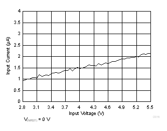
GUID-0649CF62-7F28-4037-A8B3-70010D24FF5A-low.gifFigure 6-2 Shutdown Current Consumption vs Input Voltage
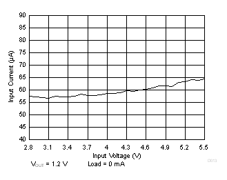
GUID-8A2F07B2-FED1-4B62-9E6A-2D0640748A9F-low.gifFigure 6-4 Active State Current Consumption vs Input Voltage, One Buck Converter Enabled in PFM Mode
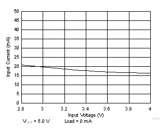
GUID-4E42DF6B-6BF3-48FE-975C-1868F9C55668-low.gifFigure 6-6 Active State Current Consumption vs Input Voltage, Boost Converter Enabled in PWM Mode
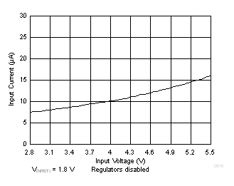
GUID-3847778B-ED4C-4DC5-BB46-2913C2E852BD-low.gifFigure 6-3 Standby Current Consumption vs Input Voltage
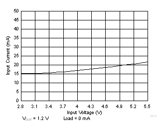
GUID-CD08C266-39E0-45A4-B509-AC8CC8F5753D-low.gifFigure 6-5 Active State Current Consumption vs Input Voltage, One Buck Converter Enabled in PWM Mode