JAJSPY3 August   2023 LV5144

PRODUCTION DATA  

  1.   1
  2. 特長
  3. アプリケーション
  4. 概要
  5. Revision History
  6. 概要 (続き)
  7. Pin Configuration and Functions
    1. 6.1 Wettable Flanks
  8. Specifications
    1. 7.1 Absolute Maximum Ratings
    2. 7.2 ESD Ratings
    3. 7.3 Recommended Operating Conditions
    4. 7.4 Thermal Information
    5. 7.5 Electrical Characteristics
    6. 7.6 Typical Characteristics
  9. Detailed Description
    1. 8.1 Overview
    2. 8.2 Functional Block Diagram
    3. 8.3 Feature Description
      1. 8.3.1  Input Range (VIN)
      2. 8.3.2  Output Voltage Setpoint and Accuracy (FB)
      3. 8.3.3  High-Voltage Bias Supply Regulator (VCC)
      4. 8.3.4  Precision Enable (EN/UVLO)
      5. 8.3.5  Power Good Monitor (PGOOD)
      6. 8.3.6  Switching Frequency (RT, SYNCIN)
        1. 8.3.6.1 Frequency Adjust
        2. 8.3.6.2 Clock Synchronization
      7. 8.3.7  Configurable Soft Start (SS/TRK)
        1. 8.3.7.1 Tracking
      8. 8.3.8  Voltage-Mode Control (COMP)
      9. 8.3.9  Gate Drivers (LO, HO)
      10. 8.3.10 Current Sensing and Overcurrent Protection (ILIM)
      11. 8.3.11 OCP Duty Cycle Limiter
    4. 8.4 Device Functional Modes
      1. 8.4.1 Shutdown Mode
      2. 8.4.2 Standby Mode
      3. 8.4.3 Active Mode
      4. 8.4.4 Diode Emulation Mode
      5. 8.4.5 Thermal Shutdown
  10. Application and Implementation
    1. 9.1 Application Information
      1. 9.1.1 Design and Implementation
      2. 9.1.2 Power Train Components
        1. 9.1.2.1 Inductor
        2. 9.1.2.2 Output Capacitors
        3. 9.1.2.3 Input Capacitors
        4. 9.1.2.4 Power MOSFETs
      3. 9.1.3 Control Loop Compensation
      4. 9.1.4 EMI Filter Design
    2. 9.2 Typical Applications
      1. 9.2.1 Design 1 – 12-A High-Efficiency Synchronous Buck DC/DC Regulator
        1. 9.2.1.1 Design Requirements
        2. 9.2.1.2 Detailed Design Procedure
        3. 9.2.1.3 Application Curves
      2. 9.2.2 Design 2 – High Density, 12-V, 8-A Rail From 48-V Telecom Power
        1. 9.2.2.1 Design Requirements
        2. 9.2.2.2 Detailed Design Procedure
        3. 9.2.2.3 Application Curves
    3. 9.3 Power Supply Recommendations
    4. 9.4 Layout
      1. 9.4.1 Layout Guidelines
        1. 9.4.1.1 Power Stage Layout
        2. 9.4.1.2 Gate Drive Layout
        3. 9.4.1.3 PWM Controller Layout
        4. 9.4.1.4 Thermal Design and Layout
        5. 9.4.1.5 Ground Plane Design
      2. 9.4.2 Layout Example
  11. 10Device and Documentation Support
    1. 10.1 Device Support
      1. 10.1.1 サード・パーティ製品に関する免責事項
      2. 10.1.2 Development Support
    2. 10.2 Documentation Support
      1. 10.2.1 Related Documentation
        1. 10.2.1.1 PCB Layout Resources
        2. 10.2.1.2 Thermal Design Resources
    3. 10.3 ドキュメントの更新通知を受け取る方法
    4. 10.4 サポート・リソース
    5. 10.5 Trademarks
    6. 10.6 静電気放電に関する注意事項
    7. 10.7 用語集
  12. 11Mechanical, Packaging, and Orderable Information

パッケージ・オプション

メカニカル・データ(パッケージ|ピン)
サーマルパッド・メカニカル・データ
発注情報

Frequency Adjust

Adjust the free-running switching frequency by using a resistor from the RT pin to AGND. The switching frequency range is from 100 kHz to 1 MHz. The frequency set resistance, RRT, is governed by Equation 3. E96 standard-value resistors for common switching frequencies are given in Table 8-1.

Equation 3. GUID-51E556B7-8328-4B29-B975-8675DAC0B8DA-low.gif
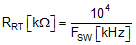
Table 8-1 Frequency Set Resistors
SWITCHING FREQUENCY (kHz)FREQUENCY SET RESISTANCE (kΩ)
100100
20049.9
25040.2
30033.2
40024.9
50020
75013.3
100010