JAJSD97 April 2017 MSP430FR5989-EP
PRODUCTION DATA.
- 1デバイスの概要
- 2改訂履歴
- 3Terminal Configuration and Functions
-
4 Specifications
- 4.1 Absolute Maximum Ratings
- 4.2 ESD Ratings
- 4.3 Recommended Operating Conditions
- 4.4 Active Mode Supply Current Into VCC Excluding External Current
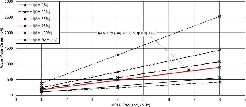
- 4.5 Typical Characteristics, Active Mode Supply Currents
- 4.6 Low-Power Mode (LPM0, LPM1) Supply Currents Into VCC Excluding External Current
- 4.7 Low-Power Mode (LPM2, LPM3, LPM4) Supply Currents (Into VCC) Excluding External Current
- 4.8 Low-Power Mode With LCD Supply Currents (Into VCC) Excluding External Current
- 4.9 Low-Power Mode LPMx.5 Supply Currents (Into VCC) Excluding External Current
- 4.10 Typical Characteristics, Low-Power Mode Supply Currents
- 4.11 Typical Characteristics, Current Consumption per Module
- 4.12 Thermal Resistance Characteristics
- 4.13
Timing and Switching Characteristics
- 4.13.1 Power Supply Sequencing
- 4.13.2 Reset Timing
- 4.13.3 Clock Specifications
- 4.13.4 Wake-up Characteristics
- 4.13.5 Peripherals
- 4.13.6 Emulation and Debug
-
5Detailed Description
- 5.1 Overview
- 5.2 CPU
- 5.3 Operating Modes
- 5.4 Interrupt Vector Table and Signatures
- 5.5 Bootloader (BSL)
- 5.6 JTAG Operation
- 5.7 FRAM
- 5.8 RAM
- 5.9 Tiny RAM
- 5.10 Memory Protection Unit Including IP Encapsulation
- 5.11
Peripherals
- 5.11.1 Digital I/O
- 5.11.2 Oscillator and Clock System (CS)
- 5.11.3 Power-Management Module (PMM)
- 5.11.4 Hardware Multiplier (MPY)
- 5.11.5 Real-Time Clock (RTC_C)
- 5.11.6 Watchdog Timer (WDT_A)
- 5.11.7 System Module (SYS)
- 5.11.8 DMA Controller
- 5.11.9 Enhanced Universal Serial Communication Interface (eUSCI)
- 5.11.10 Extended Scan Interface (ESI)
- 5.11.11 Timer_A TA0, Timer_A TA1
- 5.11.12 Timer_A TA2
- 5.11.13 Timer_A TA3
- 5.11.14 Timer_B TB0
- 5.11.15 ADC12_B
- 5.11.16 Comparator_E
- 5.11.17 CRC16
- 5.11.18 CRC32
- 5.11.19 AES256 Accelerator
- 5.11.20 True Random Seed
- 5.11.21 Shared Reference (REF_A)
- 5.11.22 LCD_C
- 5.11.23 Embedded Emulation
- 5.11.24
Input/Output Diagrams
- 5.11.24.1 Digital I/O Functionality - Ports P1 to P10
- 5.11.24.2 Capacitive Touch Functionality Ports P1 to P10 and PJ
- 5.11.24.3 Port P1 (P1.0 to P1.3) Input/Output With Schmitt Trigger
- 5.11.24.4 Port P1 (P1.4 to P1.7) Input/Output With Schmitt Trigger
- 5.11.24.5 Port P2 (P2.0 to P2.3) Input/Output With Schmitt Trigger
- 5.11.24.6 Port P2 (P2.4 to P2.7) Input/Output With Schmitt Trigger
- 5.11.24.7 Port P3 (P3.0 to P3.7) Input/Output With Schmitt Trigger
- 5.11.24.8 Port P4 (P4.0 to P4.7) Input/Output With Schmitt Trigger
- 5.11.24.9 Port P5 (P5.0 to P5.7) Input/Output With Schmitt Trigger
- 5.11.24.10 Port P6 (P6.0 to P6.6) Input/Output With Schmitt Trigger
- 5.11.24.11 Port P6 (P6.7) Input/Output With Schmitt Trigger
- 5.11.24.12 Port P7 (P7.0 to P7.7) Input/Output With Schmitt Trigger
- 5.11.24.13 Port P8 (P8.0 to P8.3) Input/Output With Schmitt Trigger
- 5.11.24.14 Port P8 (P8.4 to P8.7) Input/Output With Schmitt Trigger
- 5.11.24.15 Port P9 (P9.0 to P9.3) Input/Output With Schmitt Trigger
- 5.11.24.16 Port P9 (P9.4 to P9.7) Input/Output With Schmitt Trigger
- 5.11.24.17 Port P10 (P10.0 to P10.2) Input/Output With Schmitt Trigger
- 5.11.24.18 Port PJ (PJ.4 and PJ.5) Input/Output With Schmitt Trigger
- 5.11.24.19 Port PJ (PJ.6 and PJ.7) Input/Output With Schmitt Trigger
- 5.11.24.20 Port PJ (PJ.0 to PJ.3) JTAG Pins TDO, TMS, TCK, TDI/TCLK, Input/Output With Schmitt Trigger
- 5.12 Device Descriptors (TLV)
- 5.13 Memory
- 5.14 Identification
- 6Applications, Implementation, and Layout
- 7デバイスおよびドキュメントのサポート
- 8メカニカル、パッケージ、および注文情報
4 Specifications
4.1 Absolute Maximum Ratings(1)
over operating junction temperature range (unless otherwise noted)| MIN | MAX | UNIT | |
|---|---|---|---|
| Voltage applied at DVCC and AVCC pins to VSS | –0.3 | 4.1 | V |
| Voltage difference between DVCC and AVCC pins(2) | ±0.3 | V | |
| Voltage applied to any pin(3) | –0.3 | VCC + 0.3 V (4.1 max) |
V |
| Diode current at any device pin | ±2 | mA | |
| Storage temperature, Tstg(4) | –55 | 125 | °C |
4.2 ESD Ratings
| VALUE | UNIT | |||
|---|---|---|---|---|
| V(ESD) | Electrostatic discharge | Human-body model (HBM), per ANSI/ESDA/JEDEC JS-001(1) | ±1000 | V |
| Charged-device model (CDM), per JEDEC specification JESD22-C101(2) | ±250 | |||
4.3 Recommended Operating Conditions
Typical data are based on VCC = 3 V, TJ = 25°C unless otherwise noted.| MIN | NOM | MAX | UNIT | |||
|---|---|---|---|---|---|---|
| VCC | Supply voltage range applied at all DVCC, AVCC, and ESIDVCC pins(1) (2) (3) | 1.8(6) | 3.6 | V | ||
| VSS | Supply voltage applied at all DVSS, AVSS, and ESIDVSS pins | 0 | V | |||
| TJ | Operating junction temperature | –55 | 95 | °C | ||
| CDVCC | Capacitor value at DVCC and ESIDVCC(4) | 1–20% | µF | |||
| fSYSTEM | Processor frequency (maximum MCLK frequency)(5) | No FRAM wait states (NWAITSx = 0) | 0 | 8(8) | MHz | |
| With FRAM wait states (NWAITSx = 1)(7) | 0 | 16(9) | ||||
| fACLK | Maximum ACLK frequency | 50 | kHz | |||
| fSMCLK | Maximum SMCLK frequency | 16(9) | MHz | |||
4.4 Active Mode Supply Current Into VCC Excluding External Current
over recommended operating junction temperature (unless otherwise noted)(1) (2)| PARAMETER | EXECUTION MEMORY | VCC | FREQUENCY (fMCLK = fSMCLK) | UNIT | |||||||||
|---|---|---|---|---|---|---|---|---|---|---|---|---|---|
| 1 MHz 0 WAIT STATES (NWAITSx = 0) |
4 MHz 0 WAIT STATES (NWAITSx = 0) |
8 MHz 0 WAIT STATES (NWAITSx = 0) |
12 MHz 1 WAIT STATE (NWAITSx = 1) |
16 MHz 1 WAIT STATE (NWAITSx = 1) |
|||||||||
| TYP | MAX | TYP | MAX | TYP | MAX | TYP | MAX | TYP | MAX | ||||
| IAM, FRAM_UNI
(Unified memory)(3) |
FRAM | 3.0 V | 210 | 640 | 1220 | 1475 | 1845 | µA | |||||
| IAM, FRAM(0%)(4) (5) | FRAM 0% cache hit ratio |
3.0 V | 375 | 1290 | 2525 | 2100 | 2675 | µA | |||||
| IAM, FRAM(50%)(4) (5) | FRAM 50% cache hit ratio |
3.0 V | 240 | 745 | 1440 | 1575 | 1990 | µA | |||||
| IAM, FRAM(66%)(4) (5) | FRAM 66% cache hit ratio |
3.0 V | 200 | 560 | 1070 | 1300 | 1620 | µA | |||||
| IAM, FRAM(75%)(4) (5) | FRAM 75% cache hit ratio |
3.0 V | 170 | 255 | 480 | 890 | 1085 | 1155 | 1310 | 1420 | 1620 | µA | |
| IAM, FRAM(100%(4) (5) | FRAM 100% cache hit ratio |
3.0 V | 110 | 235 | 420 | 640 | 730 | µA | |||||
| IAM, RAM (6) (5) | RAM | 3.0 V | 130 | 320 | 585 | 890 | 1070 | µA | |||||
| IAM, RAM only (7) (5) | RAM | 3.0 V | 100 | 180 | 290 | 555 | 860 | 1040 | 1300 | µA | |||
fACLK = 32768 Hz, fMCLK = fSMCLK = fDCO at specified frequency, except for 12 MHz. For 12 MHz, fDCO = 24 MHz and fMCLK = fSMCLK = fDCO / 2.
At MCLK frequencies above 8 MHz, the FRAM requires wait states. When wait states are required, the effective MCLK frequency (fMCLK,eff) decreases. The effective MCLK frequency also depends on the cache hit ratio. SMCLK is not affected by the number of wait states or the cache hit ratio.
The following equation can be used to compute fMCLK,eff:
fMCLK,eff = fMCLK / [wait states × (1 – cache hit ratio) + 1]
For example, with 1 wait state and 75% cache hit ratio fMCKL,eff = fMCLK / [1 × (1 – 0.75) + 1] = fMCLK / 1.25.
4.5 Typical Characteristics, Active Mode Supply Currents
4.6 Low-Power Mode (LPM0, LPM1) Supply Currents Into VCC Excluding External Current
over recommended operating junction temperature (unless otherwise noted)(1) (2)| PARAMETER | VCC | FREQUENCY (fSMCLK) | UNIT | |||||||||
|---|---|---|---|---|---|---|---|---|---|---|---|---|
| 1 MHz | 4 MHz | 8 MHz | 12 MHz | 16 MHz | ||||||||
| TYP | MAX | TYP | MAX | TYP | MAX | TYP | MAX | TYP | MAX | |||
| ILPM0 | 2.2 V | 75 | 105 | 165 | 250 | 230 | µA | |||||
| 3.0 V | 85 | 120 | 115 | 175 | 260 | 240 | 275 | |||||
| ILPM1 | 2.2 V | 40 | 65 | 130 | 215 | 195 | µA | |||||
| 3.0 V | 40 | 65 | 65 | 130 | 215 | 195 | 220 | |||||
fACLK = 32768 Hz, fMCLK = 0 MHz, fSMCLK = fDCO at specified frequency, except for 12 MHz: here fDCO = 24 MHz and fSMCLK = fDCO / 2.
4.7 Low-Power Mode (LPM2, LPM3, LPM4) Supply Currents (Into VCC) Excluding External Current
over recommended ranges of supply voltage and operating junction temperature (unless otherwise noted) (1)| PARAMETER | VCC | TEMPERATURE (TJ) | UNIT | ||||||||
|---|---|---|---|---|---|---|---|---|---|---|---|
| –55°C | 25°C | 60°C | 95°C | ||||||||
| TYP | MAX | TYP | MAX | TYP | MAX | TYP | MAX | ||||
| ILPM2,XT12 | Low-power mode 2, 12-pF crystal(1) (3) (4) | 2.2 V | 0.6 | 1.2 | 3.1 | 8.8 | μA | ||||
| 3.0 V | 0.6 | 1.2 | 2.2 | 3.1 | 8.8 | 20.8 | |||||
| ILPM2,XT3.7 | Low-power mode 2, 3.7-pF crystal(1) (2) (4) | 2.2 V | 0.5 | 1.1 | 3.0 | 8.7 | μA | ||||
| 3.0 V | 0.5 | 1.1 | 3.0 | 8.7 | |||||||
| ILPM2,VLO | Low-power mode 2, VLO, includes SVS(5) | 2.2 V | 0.3 | 0.9 | 2.8 | 8.5 | μA | ||||
| 3.0 V | 0.3 | 0.9 | 2.0 | 2.8 | 8.5 | 20.5 | |||||
| ILPM3,XT12 | Low-power mode 3, 12-pF crystal, excludes SVS(1) (3) (6) | 2.2 V | 0.5 | 0.7 | 1.2 | 2.5 | μA | ||||
| 3.0 V | 0.5 | 0.7 | 1.0 | 1.2 | 2.5 | 6.4 | |||||
| ILPM3,XT3.7 | Low-power mode 3, 3.7-pF crystal, excludes SVS(1) (2) (7)
(also see Figure 4-2) |
2.2 V | 0.4 | 0.6 | 1.1 | 2.4 | μA | ||||
| 3.0 V | 0.4 | 0.6 | 1.1 | 2.4 | |||||||
| ILPM3,VLO | Low-power mode 3, VLO, excludes SVS (8) | 2.2 V | 0.3 | 0.4 | 0.9 | 2.2 | μA | ||||
| 3.0 V | 0.3 | 0.4 | 0.8 | 0.9 | 2.2 | 6.1 | |||||
| ILPM3,VLO, RAMoff | Low-power mode 3, VLO, excludes SVS, RAM powered-down completely(9) | 2.2 V | 0.3 | 0.4 | 0.8 | 2.1 | μA | ||||
| 3.0 V | 0.3 | 0.4 | 0.7 | 0.8 | 2.1 | 5.2 | |||||
| ILPM4,SVS | Low-power mode 4, includes SVS(10) | 2.2 V | 0.4 | 0.5 | 0.9 | 2.3 | μA | ||||
| 3.0 V | 0.4 | 0.5 | 0.8 | 0.9 | 2.3 | 6.2 | |||||
| ILPM4 | Low-power mode 4, excludes SVS(11) | 2.2 V | 0.2 | 0.3 | 0.7 | 2.0 | μA | ||||
| 3.0 V | 0.2 | 0.3 | 0.6 | 0.7 | 2.0 | 6.0 | |||||
| ILPM4,RAMoff | Low-power mode 4, excludes SVS, RAM powered-down completely(12) | 2.2 V | 0.2 | 0.3 | 0.7 | 1.9 | μA | ||||
| 3.0 V | 0.2 | 0.3 | 0.6 | 0.7 | 1.9 | 5.1 | |||||
| IIDLE,GroupA | Additional idle current if one or more modules from Group A (see Table 5-3) are activated in LPM3 or LPM4 | 3.0V | 0.02 | 1.18 | 2.6 | μA | |||||
| IIDLE,GroupB | Additional idle current if one or more modules from Group B (see Table 5-3) are activated in LPM3 or LPM4 | 3.0V | 0.02 | 1.15 | 2.6 | μA | |||||
| IIDLE,GroupC | Additional idle current if one or more modules from Group C (see Table 5-3) are activated in LPM3 or LPM4 | 3.0V | 0.02 | 1.5 | 2.8 | μA | |||||
| IIDLE,GroupD | Additional idle current if one or more modules from Group D (see Table 5-3) are activated in LPM3 or LPM4 | 3.0V | 0.015 | 1.4 | 2.4 | μA | |||||
Current for watchdog timer clocked by ACLK and RTC clocked by XT1 included. Current for brownout and SVS included.
CPUOFF = 1, SCG0 = 0 SCG1 = 1, OSCOFF = 0 (LPM2),
fXT1 = 32768 Hz, fACLK = fXT1, fMCLK = fSMCLK = 0 MHz
Current for watchdog timer clocked by ACLK included. RTC disabled (RTCHOLD = 1). Current for brownout and SVS included.
CPUOFF = 1, SCG0 = 0 SCG1 = 1, OSCOFF = 0 (LPM2),
fXT1 = 0 Hz, fACLK = fVLO, fMCLK = fSMCLK = 0 MHz
Current for watchdog timer clocked by ACLK and RTC clocked by XT1 included. Current for brownout included. SVS disabled (SVSHE = 0).
CPUOFF = 1, SCG0 = 1 SCG1 = 1, OSCOFF = 0 (LPM3),
fXT1 = 32768 Hz, fACLK = fXT1, fMCLK = fSMCLK = 0 MHz
Activating additional peripherals increases the current consumption due to active supply current contribution as well as due to additional idle current. See the idle currents specified for the respective peripheral groups.
Current for watchdog timer clocked by ACLK included. RTC disabled (RTCHOLD = 1). Current for brownout included. SVS disabled (SVSHE = 0).
CPUOFF = 1, SCG0 = 1 SCG1 = 1, OSCOFF = 0 (LPM3),
fXT1 = 0 Hz, fACLK = fVLO, fMCLK = fSMCLK = 0 MHz
Activating additional peripherals increases the current consumption due to active supply current contribution as well as due to additional idle current. See the idle currents specified for the respective peripheral groups.
Current for watchdog timer clocked by ACLK included. RTC disabled (RTCHOLD = 1). RAM disabled (RCCTL0 = 5A55h). Current for brownout included. SVS disabled (SVSHE = 0).
CPUOFF = 1, SCG0 = 1 SCG1 = 1, OSCOFF = 0 (LPM3),
fXT1 = 0 Hz, fACLK = fVLO, fMCLK = fSMCLK = 0 MHz
Activating additional peripherals increases the current consumption due to active supply current contribution as well as due to additional idle current. See the idle currents specified for the respective peripheral groups.
Current for brownout and SVS included (SVSHE = 1).
CPUOFF = 1, SCG0 = 1 SCG1 = 1, OSCOFF = 1 (LPM4),
fXT1 = 0 Hz, fACLK = 0 Hz, fMCLK = fSMCLK = 0 MHz
Activating additional peripherals increases the current consumption due to active supply current contribution as well as due to additional idle current. See the idle currents specified for the respective peripheral groups.
Current for brownout included. SVS disabled (SVSHE = 0).
CPUOFF = 1, SCG0 = 1 SCG1 = 1, OSCOFF = 1 (LPM4),
fXT1 = 0 Hz, fACLK = 0 Hz, fMCLK = fSMCLK = 0 MHz
Activating additional peripherals increases the current consumption due to active supply current contribution as well as due to additional idle current. See the idle currents specified for the respective peripheral groups.
Current for brownout included. SVS disabled (SVSHE = 0). RAM disabled (RCCTL0 = 5A55h).
CPUOFF = 1, SCG0 = 1 SCG1 = 1, OSCOFF = 1 (LPM4),
fXT1 = 0 Hz, fACLK = 0 Hz, fMCLK = fSMCLK = 0 MHz
Activating additional peripherals increases the current consumption due to active supply current contribution as well as due to additional idle current. See the idle currents specified for the respective peripheral groups.
4.8 Low-Power Mode With LCD Supply Currents (Into VCC) Excluding External Current
over recommended ranges of supply voltage and operating junction temperature (unless otherwise noted)| PARAMETER | VCC | TEMPERATURE (TJ) | UNIT | ||||||||
|---|---|---|---|---|---|---|---|---|---|---|---|
| –55°C | 25°C | 60°C | 95°C | ||||||||
| TYP | MAX | TYP | MAX | TYP | MAX | TYP | MAX | ||||
| ILPM3,XT12
LCD, ext. bias |
Low-power mode 3 (LPM3) current,12-pF crystal, LCD 4-mux mode, external biasing, excludes SVS(1) (2) | 3.0 V | 0.7 | 0.9 | 1.5 | 3.1 | µA | ||||
| ILPM3,XT12
LCD, int. bias |
Low-power mode 3 (LPM3) current, 12-pF crystal, LCD 4-mux mode, internal biasing, charge pump disabled, excludes SVS(1) (3) | 3.0 V | 2.0 | 2.2 | 2.9 | 2.8 | 4.4 | 9.3 | µA | ||
| ILPM3,XT12
LCD,CP |
Low-power mode 3 (LPM3) current,12-pF crystal, LCD 4-mux mode, internal biasing, charge pump enabled, 1/3 bias, excludes SVS(1) (4) | 2.2 V | 5.0 | 5.2 | 5.8 | 7.4 | µA | ||||
| 3.0 V | 4.5 | 4.7 | 5.3 | 6.9 | |||||||
CPUOFF = 1, SCG0 = 1 SCG1 = 1, OSCOFF = 0 (LPM3),
fXT1 = 32768 Hz, fACLK = fXT1, fMCLK = fSMCLK = 0 MHz
Activating additional peripherals increases the current consumption due to active supply current contribution as well as due to additional idle current - idle current of Group containing LCD module already included. See the idle currents specified for the respective peripheral groups.
Current through external resistors not included (voltage levels are supplied by test equipment).
Even segments S0, S2, ... = 0, odd segments S1, S3, ... = 1. No LCD panel load.
Even segments S0, S2, ...=0, odd segments S1, S3, ... = 1. No LCD panel load.
Even segments S0, S2, ...=0, odd segments S1, S3, ... = 1. No LCD panel load. CLCDCAP = 10 µF
4.9 Low-Power Mode LPMx.5 Supply Currents (Into VCC) Excluding External Current
over recommended ranges of supply voltage and operating junction temperature (unless otherwise noted)(1)| PARAMETER | VCC | –55°C | 25°C | 60°C | 95°C | UNIT | |||||
|---|---|---|---|---|---|---|---|---|---|---|---|
| TYP | MAX | TYP | MAX | TYP | MAX | TYP | MAX | ||||
| ILPM3.5,XT12 | Low-power mode 3.5, 12-pF crystal including SVS(1) (3) (4) | 2.2 V | 0.4 | 0.45 | 0.55 | 0.75 | μA | ||||
| 3.0 V | 0.4 | 0.45 | 0.7 | 0.55 | 0.75 | 1.6 | |||||
| ILPM3.5,XT3.7 | Low-power mode 3.5, 3.7-pF crystal excluding SVS(1) (2) (5) | 2.2 V | 0.3 | 0.35 | 0.4 | 0.65 | μA | ||||
| 3.0 V | 0.3 | 0.35 | 0.4 | 0.65 | |||||||
| ILPM4.5,SVS | Low-power mode 4.5, including SVS(6) | 2.2 V | 0.2 | 0.2 | 0.25 | 0.35 | μA | ||||
| 3.0 V | 0.2 | 0.2 | 0.4 | 0.25 | 0.35 | 0.7 | |||||
| ILPM4.5 | Low-power mode 4.5, excluding SVS(7) | 2.2 V | 0.02 | 0.02 | 0.03 | 0.14 | μA | ||||
| 3.0 V | 0.02 | 0.02 | 0.03 | 0.13 | 0.5 | ||||||
Current for RTC clocked by XT1 included. Current for brownout and SVS included (SVSHE = 1). Core regulator disabled.
PMMREGOFF = 1, CPUOFF = 1, SCG0 = 1 SCG1 = 1, OSCOFF = 1 (LPMx.5),
fXT1 = 32768 Hz, fACLK = fXT1, fMCLK = fSMCLK = 0 MHz
Current for RTC clocked by XT1 included.Current for brownout included. SVS disabled (SVSHE = 0). Core regulator disabled.
PMMREGOFF = 1, CPUOFF = 1, SCG0 = 1 SCG1 = 1, OSCOFF = 1 (LPMx.5),
fXT1 = 32768 Hz, fACLK = fXT1, fMCLK = fSMCLK = 0 MHz
Current for brownout and SVS included (SVSHE = 1). Core regulator disabled.
PMMREGOFF = 1, CPUOFF = 1, SCG0 = 1 SCG1 = 1, OSCOFF = 1 (LPMx.5),
fXT1 = 0 Hz, fACLK = 0 Hz, fMCLK = fSMCLK = 0 MHz
Current for brownout included. SVS disabled (SVSHE = 0). Core regulator disabled.
PMMREGOFF = 1, CPUOFF = 1, SCG0 = 1 SCG1 = 1, OSCOFF = 1 (LPMx.5),
fXT1 = 0 Hz, fACLK = 0 Hz, fMCLK = fSMCLK = 0 MHz
4.10 Typical Characteristics, Low-Power Mode Supply Currents
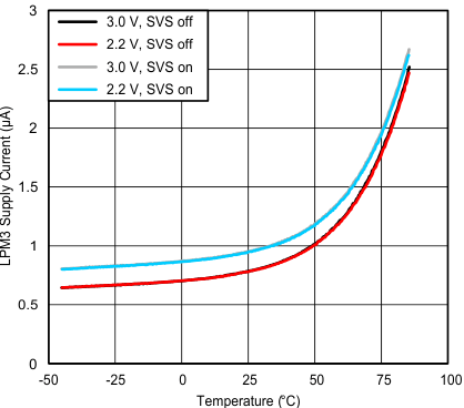 Figure 4-2 LPM3 Supply Current vs Temperature (LPM3, XT3.7)
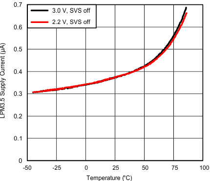 Figure 4-4 LPM3.5 Supply Current vs Temperature (LPM3.5, XT3.7)
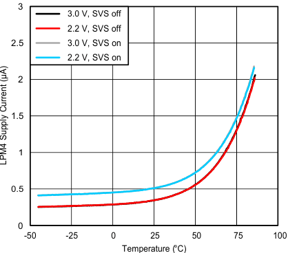 Figure 4-3 LPM4 Supply Current vs Temperature (LPM4, SVS)
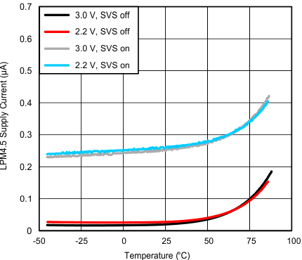 Figure 4-5 LPM4.5 Supply Current vs Temperature (LPM4.5)
4.11 Typical Characteristics, Current Consumption per Module(1)
| MODULE | TEST CONDITIONS | REFERENCE CLOCK | MIN | TYP | MAX | UNIT |
|---|---|---|---|---|---|---|
| Timer_A | Module input clock | 3 | μA/MHz | |||
| Timer_B | Module input clock | 5 | μA/MHz | |||
| eUSCI_A | UART mode | Module input clock | 5.5 | μA/MHz | ||
| eUSCI_A | SPI mode | Module input clock | 3.5 | μA/MHz | ||
| eUSCI_B | SPI mode | Module input clock | 3.5 | μA/MHz | ||
| eUSCI_B | I2C mode, 100 kbaud | Module input clock | 3.5 | μA/MHz | ||
| RTC_C | 32 kHz | 100 | nA | |||
| MPY | Only from start to end of operation | MCLK | 25 | μA/MHz | ||
| AES | Only from start to end of operation | MCLK | 21 | μA/MHz | ||
| CRC16 | Only from start to end of operation | MCLK | 2.5 | μA/MHz | ||
| CRC32 | Only from start to end of operation | MCLK | 2.5 | μA/MHz |
4.12 Thermal Resistance Characteristics
| THERMAL METRIC(1) | MSP430FR5989-EP | UNIT | ||
|---|---|---|---|---|
| RGC (VQFN) | ||||
| 64 Pins | ||||
| RθJA | Junction-to-ambient thermal resistance, still air(2) | 29.2 | °C/W | |
| RθJC(top) | Junction-to-case (top) thermal resistance(3) | 13.9 | °C/W | |
| RθJB | Junction-to-board thermal resistance(5) | 8.1 | °C/W | |
| ΨJT | Junction-to-top thermal characterization parameter | 8.0 | °C/W | |
| ΨJB | Junction-to-board thermal characterization parameter | 0.2 | °C/W | |
| RθJC(bot) | Junction-to-case (bottom) thermal resistance(4) | 1.0 | °C/W | |
4.13 Timing and Switching Characteristics
4.13.1 Power Supply Sequencing
TI recommends powering the AVCC, DVCC, and ESIDVCC pins from the same source. At a minimum, during power up, power down, and device operation, the voltage difference between AVCC, DVCC, and ESIDVCC must not exceed the limits specified in Absolute Maximum Ratings. Exceeding the specified limits may cause malfunction of the device including erroneous writes to RAM and FRAM.
At power up, the device does not start executing code before the supply voltage reached VSVSH+ if the supply rises monotonically to this level.
Table 4-1 lists the power ramp requirements.
Table 4-1 Brownout and Device Reset Power Ramp Requirements
over recommended ranges of supply voltage and operating junction temperature (unless otherwise noted)| PARAMETER | TEST CONDITIONS | MIN | MAX | UNIT | |
|---|---|---|---|---|---|
| VVCC_BOR– | Brownout power-down level(1)(2) | | dDVCC/dt | < 3 V/s(3) | 0.7 | 1.66 | V |
| | dDVCC/dt | > 300 V/s(3) | 0 | ||||
| VVCC_BOR+ | Brownout power-up level(2) | | dDVCC/dt | < 3 V/s(4) | 0.79 | 1.68 | V |
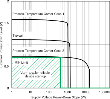 Figure 4-6 Brownout Power-Down Level vs Supply Voltage Down Slope
Table 4-2 lists the characteristics of the SVS.
Table 4-2 SVS
over recommended ranges of supply voltage and operating junction temperature (unless otherwise noted)| PARAMETER | TEST CONDITIONS | MIN | TYP | MAX | UNIT | |
|---|---|---|---|---|---|---|
| ISVSH,LPM | SVSH current consumption, low-power modes | 170 | 300 | nA | ||
| VSVSH- | SVSH power-down level | 1.74 | 1.81 | 1.86 | V | |
| VSVSH+ | SVSH power-up level | 1.76 | 1.88 | 1.99 | V | |
| VSVSH_hys | SVSH hysteresis | 40 | 120 | mV | ||
| tPD,SVSH, AM | SVSH propagation delay, active mode | dVVcc/dt = –10 mV/µs | 10 | µs | ||
4.13.2 Reset Timing
Table 4-3 lists the input requirements for the RST signal.
Table 4-3 Reset Input
over recommended ranges of supply voltage and operating junction temperature (unless otherwise noted)| PARAMETER | VCC | MIN | MAX | UNIT | |
|---|---|---|---|---|---|
| t(RST) | External reset pulse duration on RST(1) | 2.2 V, 3.0 V | 2 | µs | |
4.13.3 Clock Specifications
Table 4-4 lists the characteristics of the LFXT.
Table 4-4 Low-Frequency Crystal Oscillator, LFXT(4)
over recommended ranges of supply voltage and operating junction temperature (unless otherwise noted)| PARAMETER | TEST CONDITIONS | VCC | MIN | TYP | MAX | UNIT | |
|---|---|---|---|---|---|---|---|
| IVCC.LFXT | Current consumption | fOSC = 32768 Hz, LFXTBYPASS = 0, LFXTDRIVE = {0}, TJ = 25°C, CL,eff = 3.7 pF, ESR ≈ 44 kΩ |
3.0 V | 180 | nA | ||
| fOSC = 32768 Hz, LFXTBYPASS = 0, LFXTDRIVE = {1}, TJ = 25°C, CL,eff = 6 pF, ESR ≈ 40 kΩ |
3.0 V | 185 | |||||
| fOSC = 32768 Hz, LFXTBYPASS = 0, LFXTDRIVE = {2}, TJ = 25°C, CL,eff = 9 pF, ESR ≈ 40 kΩ |
3.0 V | 225 | |||||
| fOSC = 32768 Hz, LFXTBYPASS = 0, LFXTDRIVE = {3}, TJ = 25°C, CL,eff = 12.5 pF, ESR ≈ 40 kΩ |
3.0 V | 330 | |||||
| fLFXT | LFXT oscillator crystal frequency | LFXTBYPASS = 0 | 32768 | Hz | |||
| DCLFXT | LFXT oscillator duty cycle | Measured at ACLK, fLFXT = 32768 Hz |
30% | 70% | |||
| fLFXT,SW | LFXT oscillator logic-level square-wave input frequency | LFXTBYPASS = 1(5) (8) | 10.5 | 32.768 | 50 | kHz | |
| DCLFXT, SW | LFXT oscillator logic-level square-wave input duty cycle | LFXTBYPASS = 1 | 30% | 70% | |||
| OALFXT | Oscillation allowance for LF crystals(9) | LFXTBYPASS = 0, LFXTDRIVE = {1}, fLFXT = 32768 Hz, CL,eff = 6 pF |
210 | kΩ | |||
| LFXTBYPASS = 0, LFXTDRIVE = {3}, fLFXT = 32768 Hz, CL,eff = 12.5 pF |
300 | ||||||
| CLFXIN | Integrated load capacitance at LFXIN terminal(6) (7) | 2 | pF | ||||
| CLFXOUT | Integrated load capacitance at LFXOUT terminal(6) (7) | 2 | pF | ||||
| tSTART,LFXT | Start-up time(2) | fOSC = 32768 Hz, LFXTBYPASS = 0, LFXTDRIVE = {0}, TJ = 25°C, CL,eff = 3.7 pF |
3.0 V | 800 | ms | ||
| fOSC = 32768 Hz, LFXTBYPASS = 0, LFXTDRIVE = {3}, TJ = 25°C, CL,eff = 12.5 pF |
3.0 V | 1000 | |||||
| fFault,LFXT | Oscillator fault frequency(3) (1) | 0 | 3500 | Hz | |||
- Keep the trace between the device and the crystal as short as possible.
- Design a good ground plane around the oscillator pins.
- Prevent crosstalk from other clock or data lines into oscillator pins LFXIN and LFXOUT.
- Avoid running PCB traces underneath or adjacent to the LFXIN and LFXOUT pins.
- Use assembly materials and processes that avoid any parasitic load on the oscillator LFXIN and LFXOUT pins.
- If conformal coating is used, ensure that it does not induce capacitive or resistive leakage between the oscillator pins.
- For LFXTDRIVE = {0}, CL,eff = 3.7 pF.
- For LFXTDRIVE = {1}, CL,eff = 6 pF
- For LFXTDRIVE = {2}, 6 pF ≤ CL,eff ≤ 9 pF
- For LFXTDRIVE = {3}, 9 pF ≤ CL,eff ≤ 12.5 pF
Table 4-5 lists the characteristics of the HFXT.
Table 4-5 High-Frequency Crystal Oscillator, HFXT(5)
over recommended ranges of supply voltage and operating junction temperature (unless otherwise noted)| PARAMETER | TEST CONDITIONS | VCC | MIN | TYP | MAX | UNIT | |
|---|---|---|---|---|---|---|---|
| IDVCC.HFXT | HFXT oscillator crystal current HF mode at typical ESR | fOSC = 4 MHz, HFXTBYPASS = 0, HFXTDRIVE = 0, HFFREQ = 1(8) TJ = 25°C, CL,eff = 18 pF, Typical ESR, Cshunt |
3.0 V | 75 | μA | ||
| fOSC = 8 MHz, HFXTBYPASS = 0, HFXTDRIVE = 1, HFFREQ = 1, TJ = 25°C, CL,eff = 18 pF, Typical ESR, Cshunt |
120 | ||||||
| fOSC = 16 MHz, HFXTBYPASS = 0, HFXTDRIVE = 2, HFFREQ = 2, TJ = 25°C, CL,eff = 18 pF, Typical ESR, Cshunt |
190 | ||||||
| fOSC = 24 MHz, HFXTBYPASS = 0, HFXTDRIVE = 3, HFFREQ = 3, TJ = 25°C, CL,eff = 18 pF, Typical ESR, Cshunt |
250 | ||||||
| fHFXT | HFXT oscillator crystal frequency, crystal mode | HFXTBYPASS = 0, HFFREQ = 1(8)(7) | 4 | 8 | MHz | ||
| HFXTBYPASS = 0, HFFREQ = 2(7) | 8.01 | 16 | |||||
| HFXTBYPASS = 0, HFFREQ = 3(7) | 16.01 | 24 | |||||
| DCHFXT | HFXT oscillator duty cycle | Measured at SMCLK, fHFXT = 16 MHz | 40% | 50% | 60% | ||
| fHFXT,SW | HFXT oscillator logic-level square-wave input frequency, bypass mode | HFXTBYPASS = 1, HFFREQ = 0(6)(7) | 0.9 | 4 | MHz | ||
| HFXTBYPASS = 1, HFFREQ = 1(6)(7) | 4.01 | 8 | |||||
| HFXTBYPASS = 1, HFFREQ = 2(6)(7) | 8.01 | 16 | |||||
| HFXTBYPASS = 1, HFFREQ = 3(6)(7) | 16.01 | 24 | |||||
| DCHFXT, SW | HFXT oscillator logic-level square-wave input duty cycle | HFXTBYPASS = 1 | 40% | 60% | |||
| tSTART,HFXT | Start-up time(9) | fOSC = 4 MHz, HFXTBYPASS = 0, HFXTDRIVE = 0, HFFREQ = 1, TJ = 25°C, CL,eff = 16 pF |
3.0 V | 1.6 | ms | ||
| fOSC = 24 MHz , HFXTBYPASS = 0, HFXTDRIVE = 3, HFFREQ = 3, TJ = 25°C, CL,eff = 16 pF |
3.0 V | 0.6 | |||||
| CHFXIN | Integrated load capacitance at HFXIN terminaI(1) (2) | 2 | pF | ||||
| CHFXOUT | Integrated load capacitance at HFXOUT terminaI(1) (2) | 2 | pF | ||||
| fFault,HFXT | Oscillator fault frequency(4) (3) | 0 | 800 | kHz | |||
- Keep the traces between the device and the crystal as short as possible.
- Design a good ground plane around the oscillator pins.
- Prevent crosstalk from other clock or data lines into oscillator pins HFXIN and HFXOUT.
- Avoid running PCB traces underneath or adjacent to the HFXIN and HFXOUT pins.
- Use assembly materials and processes that avoid any parasitic load on the oscillator HFXIN and HFXOUT pins.
- If conformal coating is used, ensure that it does not induce capacitive or resistive leakage between the oscillator pins.
Table 4-6 lists the characteristics of the DCO.
Table 4-6 DCO
over recommended ranges of supply voltage and operating junction temperature (unless otherwise noted)| PARAMETER | TEST CONDITIONS | VCC | MIN | TYP | MAX | UNIT | |
|---|---|---|---|---|---|---|---|
| fDCO1 | DCO frequency range 1 MHz, trimmed | Measured at SMCLK, divide by 1, DCORSEL = 0, DCOFSEL = 0, DCORSEL = 1, DCOFSEL = 0 |
1 | ±3.5% | MHz | ||
| fDCO2.7 | DCO frequency range 2.7 MHz, trimmed | Measured at SMCLK, divide by 1, DCORSEL = 0, DCOFSEL = 1 |
2.667 | ±3.5% | MHz | ||
| fDCO3.5 | DCO frequency range 3.5 MHz, trimmed | Measured at SMCLK, divide by 1, DCORSEL = 0, DCOFSEL = 2 |
3.5 | ±3.5% | MHz | ||
| fDCO4 | DCO frequency range 4 MHz, trimmed | Measured at SMCLK, divide by 1, DCORSEL = 0, DCOFSEL = 3 |
4 | ±3.5% | MHz | ||
| fDCO5.3 | DCO frequency range 5.3 MHz, trimmed | Measured at SMCLK, divide by 1, DCORSEL = 0, DCOFSEL = 4, DCORSEL = 1, DCOFSEL = 1 |
5.333 | ±3.5% | MHz | ||
| fDCO7 | DCO frequency range 7 MHz, trimmed | Measured at SMCLK, divide by 1, DCORSEL = 0, DCOFSEL = 5, DCORSEL = 1, DCOFSEL = 2 |
7 | ±3.5% | MHz | ||
| fDCO8 | DCO frequency range 8 MHz, trimmed | Measured at SMCLK, divide by 1, DCORSEL = 0, DCOFSEL = 6, DCORSEL = 1, DCOFSEL = 3 |
8 | ±3.5% | MHz | ||
| fDCO16 | DCO frequency range 16 MHz, trimmed | Measured at SMCLK, divide by 1, DCORSEL = 1, DCOFSEL = 4 |
16 | ±3.5%(2) | MHz | ||
| fDCO21 | DCO frequency range 21 MHz, trimmed | Measured at SMCLK, divide by 2, DCORSEL = 1, DCOFSEL = 5 |
21 | ±3.5%(2) | MHz | ||
| fDCO24 | DCO frequency range 24 MHz, trimmed | Measured at SMCLK, divide by 2, DCORSEL = 1, DCOFSEL = 6 |
24 | ±3.5%(2) | MHz | ||
| fDCO,DC | Duty cycle | Measured at SMCLK, divide by 1, no external divide, all DCORSEL/DCOFSEL settings except DCORSEL = 1, DCOFSEL = 5 and DCORSEL = 1, DCOFSEL = 6 |
48% | 50% | 52% | ||
| tDCO, JITTER | DCO jitter | Based on fsignal = 10 kHz and DCO used for 12-bit SAR ADC sampling source. This achieves >74 dB SNR due to jitter (that is, it is limited by ADC performance). | 2 | 3 | ns | ||
| dfDCO/dT | DCO temperature drift(1) | 3.0 V | 0.01 | %/°C | |||
Table 4-7 lists the characteristics of the VLO.
Table 4-7 Internal Very-Low-Power Low-Frequency Oscillator (VLO)
over recommended ranges of supply voltage and operating junction temperature (unless otherwise noted)| PARAMETER | TEST CONDITIONS | VCC | MIN | TYP | MAX | UNIT | |
|---|---|---|---|---|---|---|---|
| IVLO | Current consumption | 100 | nA | ||||
| fVLO | VLO frequency | Measured at ACLK | 5 | 9.9 | 15 | kHz | |
| dfVLO/dT | VLO frequency temperature drift | Measured at ACLK(1) | 0.2 | %/°C | |||
| dfVLO/dVCC | VLO frequency supply voltage drift | Measured at ACLK(2) | 0.7 | %/V | |||
| fVLO,DC | Duty cycle | Measured at ACLK | 40% | 50% | 60% | ||
Table 4-8 lists the characteristics of the MODOSC.
Table 4-8 Module Oscillator (MODOSC)
over recommended ranges of supply voltage and operating junction temperature (unless otherwise noted)| PARAMETER | TEST CONDITIONS | MIN | TYP | MAX | UNIT | |
|---|---|---|---|---|---|---|
| IMODOSC | Current consumption | Enabled | 25 | μA | ||
| fMODOSC | MODOSC frequency | 4.0 | 4.8 | 5.4 | MHz | |
| fMODOSC/dT | MODOSC frequency temperature drift(1) | 0.08 | %/℃ | |||
| fMODOSC/dVCC | MODOSC frequency supply voltage drift(2) | 1.4 | %/V | |||
| DCMODOSC | Duty cycle | Measured at SMCLK, divide by 1 | 40% | 50% | 60% | |
4.13.4 Wake-up Characteristics
Table 4-9 lists the wake-up times.
Table 4-9 Wake-up Times From Low-Power Modes and Reset
over recommended ranges of supply voltage and operating junction temperature (unless otherwise noted)| PARAMETER | TEST CONDITIONS | VCC | MIN | TYP | MAX | UNIT | |
|---|---|---|---|---|---|---|---|
| tWAKE-UP FRAM | (Additional) wake-up time to activate the FRAM in AM if previously disabled by the FRAM controller or from an LPM if immediate activation is selected for wakeup | 6 | 10 | μs | |||
| tWAKE-UP LPM0 | Wake-up time from LPM0 to active mode(1) | 2.2 V, 3.0 V | 400 + 1.5 / fDCO | ns | |||
| tWAKE-UP LPM1 | Wake-up time from LPM1 to active mode(1) | 2.2 V, 3.0 V | 6 | μs | |||
| tWAKE-UP LPM2 | Wake-up time from LPM2 to active mode(1) | 2.2 V, 3.0 V | 6 | μs | |||
| tWAKE-UP LPM3 | Wake-up time from LPM3 to active mode(1) | 2.2 V, 3.0 V | 7 | 10 | μs | ||
| tWAKE-UP LPM4 | Wake-up time from LPM4 to active mode(1) | 2.2 V, 3.0 V | 7 | 10 | μs | ||
| tWAKE-UP LPM3.5 | Wake-up time from LPM3.5 to active mode(2) | 2.2 V, 3.0 V | 250 | 375 | μs | ||
| tWAKE-UP LPM4.5 | Wake-up time from LPM4.5 to active mode(2) | SVSHE = 1 | 2.2 V, 3.0 V | 250 | 375 | μs | |
| SVSHE = 0 | 2.2 V, 3.0 V | 1 | 1.5 | ms | |||
| tWAKE-UP-RST | Wake-up time from a RST pin triggered reset to active mode(2) | 2.2 V, 3.0 V | 318 | 400 | μs | ||
| tWAKE-UP-BOR | Wake-up time from power-up to active mode (2) | 2.2 V, 3.0 V | 1 | 1.5 | ms | ||
Table 4-10 lists the typical charge consumed during wakeup from various low-power modes.
Table 4-10 Typical Wake-up Charge(1)
also see Figure 4-7 and Figure 4-8| PARAMETER | TEST CONDITIONS | MIN | TYP | MAX | UNIT | |
|---|---|---|---|---|---|---|
| QWAKE-UP FRAM | Charge used for activating the FRAM in AM or during wake-up from LPM0 if previously disabled by the FRAM controller. | 15.1 | nAs | |||
| QWAKE-UP LPM0 | Charge used for wake-up from LPM0 to active mode (with FRAM active) | 4.4 | nAs | |||
| QWAKE-UP LPM1 | Charge used for wake-up from LPM1 to active mode (with FRAM active) | 15.1 | nAs | |||
| QWAKE-UP LPM2 | Charge used for wake-up from LPM2 to active mode (with FRAM active) | 15.3 | nAs | |||
| QWAKE-UP LPM3 | Charge used for wake-up from LPM3 to active mode (with FRAM active) | 16.5 | nAs | |||
| QWAKE-UP LPM4 | Charge used for wake-up from LPM4 to active mode (with FRAM active) | 16.5 | nAs | |||
| QWAKE-UP LPM3.5 | Charge used for wake-up from LPM3.5 to active mode(2) | 76 | nAs | |||
| QWAKE-UP LPM4.5 | Charge used for wake-up from LPM4.5 to active mode(2) | SVSHE = 1 | 77 | nAs | ||
| SVSHE = 0 | 77.5 | |||||
| QWAKE-UP-RESET | Charge used for reset from RST or BOR event to active mode(2) | 75 | nAs | |||
4.13.4.1 Typical Characteristics, Average LPM Currents vs Wake-up Frequency
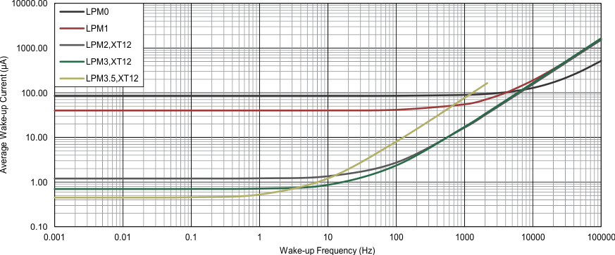
NOTE:
The average wake-up current does not include the energy required in active mode; for example, for an interrupt service routine or to reconfigure the device.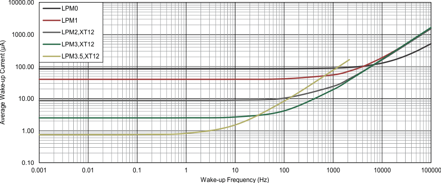
NOTE:
The average wake-up current does not include the energy required in active mode; for example, for an interrupt service routine or to reconfigure the device.4.13.5 Peripherals
4.13.5.1 Digital I/Os
Table 4-11 lists the characteristics of the digital inputs.
Table 4-11 Digital Inputs
over recommended ranges of supply voltage and operating junction temperature (unless otherwise noted)| PARAMETER | TEST CONDITIONS | VCC | MIN | TYP | MAX | UNIT | |
|---|---|---|---|---|---|---|---|
| VIT+ | Positive-going input threshold voltage | 2.2 V | 1.2 | 1.65 | V | ||
| 3.0 V | 1.65 | 2.25 | |||||
| VIT– | Negative-going input threshold voltage | 2.2 V | 0.55 | 1.00 | V | ||
| 3.0 V | 0.75 | 1.35 | |||||
| Vhys | Input voltage hysteresis (VIT+ – VIT–) | 2.2 V | 0.44 | 0.98 | V | ||
| 3.0 V | 0.60 | 1.30 | |||||
| RPull | Pullup or pulldown resistor | For pullup: VIN = VSS
For pulldown: VIN = VCC |
20 | 35 | 50 | kΩ | |
| CI,dig | Input capacitance, digital only port pins | VIN = VSS or VCC | 3 | pF | |||
| CI,ana | Input capacitance, port pins with shared analog functions(1) | VIN = VSS or VCC | 5 | pF | |||
| Ilkg(Px.y) | High-impedance input leakage current | See (2) (3) | 2.2 V, 3.0 V | –20 | +20 | nA | |
| t(int) | External interrupt timing (external trigger pulse duration to set interrupt flag)(4) | Ports with interrupt capability (see and Section 3.2) | 2.2 V, 3.0 V | 20 | ns | ||
| t(RST) | External reset pulse duration on RST(5) | 2.2 V, 3.0 V | 2 | µs | |||
Table 4-12 lists the characteristics of the digital outputs.
Table 4-12 Digital Outputs
over recommended ranges of supply voltage and operating junction temperature (unless otherwise noted)| PARAMETER | TEST CONDITIONS | VCC | MIN | TYP | MAX | UNIT | |
|---|---|---|---|---|---|---|---|
| VOH | High-level output voltage | I(OHmax) = –1 mA(1) | 2.2 V | VCC – 0.25 | VCC | V | |
| I(OHmax) = –3 mA(2) | VCC – 0.60 | VCC | |||||
| I(OHmax) = –2 mA(1) | 3.0 V | VCC – 0.25 | VCC | ||||
| I(OHmax) = –6 mA(2) | VCC – 0.60 | VCC | |||||
| VOL | Low-level output voltage | I(OLmax) = 1 mA(1) | 2.2 V | VSS | VSS + 0.25 | V | |
| I(OLmax) = 3 mA(2) | VSS | VSS + 0.60 | |||||
| I(OLmax) = 2 mA(1) | 3.0 V | VSS | VSS + 0.25 | ||||
| I(OLmax) = 6 mA(2) | VSS | VSS + 0.60 | |||||
| fPx.y | Port output frequency (with load)(5) | CL = 20 pF, RL (3) (4) | 2.2 V | 16 | MHz | ||
| 3.0 V | 16 | ||||||
| fPort_CLK | Clock output frequency(5) | ACLK, MCLK, or SMCLK at configured output port CL = 20 pF(4) |
2.2 V | 16 | MHz | ||
| 3.0 V | 16 | ||||||
| trise,dig | Port output rise time, digital only port pins | CL = 20 pF | 2.2 V | 4 | 15 | ns | |
| 3.0 V | 3 | 15 | |||||
| tfall,dig | Port output fall time, digital only port pins | CL = 20 pF | 2.2 V | 4 | 15 | ns | |
| 3.0 V | 3 | 15 | |||||
| trise,ana | Port output rise time, port pins with shared analog functions | CL = 20 pF | 2.2 V | 6 | 15 | ns | |
| 3.0 V | 4 | 15 | |||||
| tfall,ana | Port output fall time, port pins with shared analog functions | CL = 20 pF | 2.2 V | 6 | 15 | ns | |
| 3.0 V | 4 | 15 | |||||
4.13.5.1.1 Typical Characteristics, Digital Outputs at 3.0 V and 2.2 V
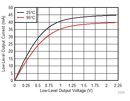
| VCC = 2.2 V |
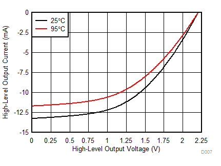
| VCC = 2.2 V |
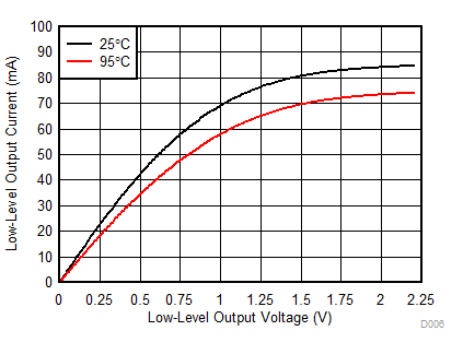
| VCC = 3.0 V |
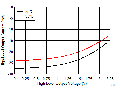
| VCC = 3.0 V |
Table 4-13 lists the frequencies of the pin oscillator.
Table 4-13 Pin-Oscillator Frequency, Ports Px
over recommended ranges of supply voltage and operating junction temperature (unless otherwise noted) (see Section 4.13.5.1.2)| PARAMETER | TEST CONDITIONS | VCC | MIN | TYP | MAX | UNIT | |
|---|---|---|---|---|---|---|---|
| foPx.y | Pin-oscillator frequency | Px.y, CL = 10 pF(1) | 3.0 V | 1200 | kHz | ||
| Px.y, CL = 20 pF(1) | 3.0 V | 650 | kHz | ||||
4.13.5.1.2 Typical Characteristics, Pin-Oscillator Frequency
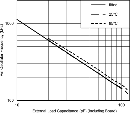
| VCC = 2.2 V | One output active at a time. | |
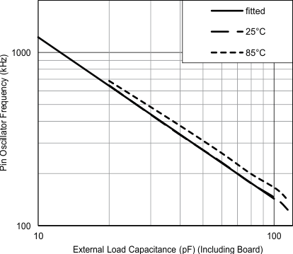
| VCC = 3.0 V | One output active at a time. | |
4.13.5.2 Timer_A and Timer_B
Table 4-14 lists the characteristics of the Timer_A.
Table 4-14 Timer_A
over recommended ranges of supply voltage and operating junction temperature (unless otherwise noted)| PARAMETER | TEST CONDITIONS | VCC | MIN | TYP | MAX | UNIT | |
|---|---|---|---|---|---|---|---|
| fTA | Timer_A input clock frequency | Internal: SMCLK or ACLK, External: TACLK, Duty cycle = 50% ±10% |
2.2 V, 3.0 V | 16 | MHz | ||
| tTA,cap | Timer_A capture timing | All capture inputs, minimum pulse duration required for capture | 2.2 V, 3.0 V | 20 | ns | ||
Table 4-15 lists the characteristics of the Timer_B.
Table 4-15 Timer_B
over recommended ranges of supply voltage and operating junction temperature (unless otherwise noted)| PARAMETER | TEST CONDITIONS | VCC | MIN | TYP | MAX | UNIT | |
|---|---|---|---|---|---|---|---|
| fTB | Timer_B input clock frequency | Internal: SMCLK or ACLK, External: TBCLK, Duty cycle = 50% ±10% |
2.2 V, 3.0 V | 16 | MHz | ||
| tTB,cap | Timer_B capture timing | All capture inputs, minimum pulse duration required for capture | 2.2 V, 3.0 V | 20 | ns | ||
4.13.5.3 eUSCI
Table 4-16 lists the supported clock frequencies of the eUSCI in UART mode.
Table 4-16 eUSCI (UART Mode) Clock Frequency
| PARAMETER | TEST CONDITIONS | MIN | MAX | UNIT | |
|---|---|---|---|---|---|
| feUSCI | eUSCI input clock frequency | Internal: SMCLK or ACLK, External: UCLK, Duty cycle = 50% ±10% |
16 | MHz | |
| fBITCLK | BITCLK clock frequency (equals baud rate in MBaud) |
4 | MHz | ||
Table 4-17 lists the characteristics of the eUSCI in UART mode.
Table 4-17 eUSCI (UART Mode)
over recommended ranges of supply voltage and operating junction temperature (unless otherwise noted)| PARAMETER | TEST CONDITIONS | VCC | MIN | TYP | MAX | UNIT | |
|---|---|---|---|---|---|---|---|
| tt | UART receive deglitch time(1) | UCGLITx = 0 | 2.2 V, 3.0 V | 5 | 30 | ns | |
| UCGLITx = 1 | 20 | 90 | |||||
| UCGLITx = 2 | 35 | 160 | |||||
| UCGLITx = 3 | 50 | 220 | |||||
Table 4-18 lists the supported clock frequencies of the eUSCI in SPI master mode.
Table 4-18 eUSCI (SPI Master Mode) Clock Frequency
| PARAMETER | TEST CONDITIONS | MIN | MAX | UNIT | |
|---|---|---|---|---|---|
| feUSCI | eUSCI input clock frequency | Internal: SMCLK or ACLK, Duty cycle = 50% ±10% |
16 | MHz | |
Table 4-19 lists the characteristics of the eUSCI in SPI master mode.
Table 4-19 eUSCI (SPI Master Mode)
over recommended ranges of supply voltage and operating junction temperature (unless otherwise noted)(1)| PARAMETER | TEST CONDITIONS | VCC | MIN | TYP | MAX | UNIT | |
|---|---|---|---|---|---|---|---|
| tSTE,LEAD | STE lead time, STE active to clock | UCSTEM = 1, UCMODEx = 01 or 10 |
1 | UCxCLK cycles | |||
| tSTE,LAG | STE lag time, last clock to STE inactive | UCSTEM = 1, UCMODEx = 01 or 10 |
1 | UCxCLK cycles | |||
| tSTE,ACC | STE access time, STE active to SIMO data out | UCSTEM = 0, UCMODEx = 01 or 10 |
2.2 V, 3.0 V | 60 | ns | ||
| tSTE,DIS | STE disable time, STE inactive to SOMI high impedance | UCSTEM = 0, UCMODEx = 01 or 10 |
2.2 V, 3.0 V | 80 | ns | ||
| tSU,MI | SOMI input data setup time | 2.2 V | 40 | ns | |||
| 3.0 V | 40 | ||||||
| tHD,MI | SOMI input data hold time | 2.2 V | 0 | ns | |||
| 3.0 V | 0 | ||||||
| tVALID,MO | SIMO output data valid time(2) | UCLK edge to SIMO valid, CL = 20 pF |
2.2 V | 10 | ns | ||
| 3.0 V | 10 | ||||||
| tHD,MO | SIMO output data hold time(3) | CL = 20 pF | 2.2 V | 0 | ns | ||
| 3.0 V | 0 | ||||||
For the slave parameters tSU,SI(Slave) and tVALID,SO(Slave), see the SPI parameters of the attached slave.
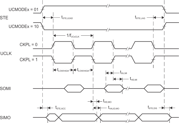 Figure 4-15 SPI Master Mode, CKPH = 0
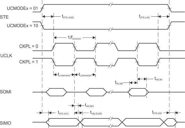 Figure 4-16 SPI Master Mode, CKPH = 1
Table 4-20 lists the characteristics of the eUSCI in SPI slave mode.
Table 4-20 eUSCI (SPI Slave Mode)
over recommended ranges of supply voltage and operating junction temperature (unless otherwise noted)(1)| PARAMETER | TEST CONDITIONS | VCC | MIN | MAX | UNIT | |
|---|---|---|---|---|---|---|
| tSTE,LEAD | STE lead time, STE active to clock | 2.2 V | 45 | ns | ||
| 3.0 V | 40 | |||||
| tSTE,LAG | STE lag time, Last clock to STE inactive | 2.2 V | 2 | ns | ||
| 3.0 V | 3 | |||||
| tSTE,ACC | STE access time, STE active to SOMI data out | 2.2 V | 45 | ns | ||
| 3.0 V | 40 | |||||
| tSTE,DIS | STE disable time, STE inactive to SOMI high impedance | 2.2 V | 50 | ns | ||
| 3.0 V | 45 | |||||
| tSU,SI | SIMO input data setup time | 2.2 V | 4 | ns | ||
| 3.0 V | 4 | |||||
| tHD,SI | SIMO input data hold time | 2.2 V | 7 | ns | ||
| 3.0 V | 7 | |||||
| tVALID,SO | SOMI output data valid time(2) | UCLK edge to SOMI valid, CL = 20 pF |
2.2 V | 35 | ns | |
| 3.0 V | 35 | |||||
| tHD,SO | SOMI output data hold time(3) | CL = 20 pF | 2.2 V | 0 | ns | |
| 3.0 V | 0 | |||||
For the master parameters tSU,MI(Master) and tVALID,MO(Master), see the SPI parameters of the attached master.
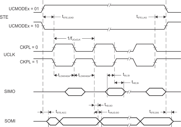 Figure 4-17 SPI Slave Mode, CKPH = 0
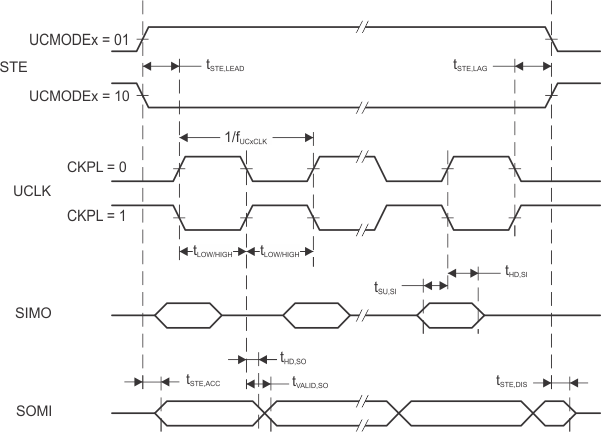 Figure 4-18 SPI Slave Mode, CKPH = 1
Table 4-21 lists the characteristics of the eUSCI in I2C mode.
Table 4-21 eUSCI (I2C Mode)
over recommended ranges of supply voltage and operating junction temperature (unless otherwise noted) (see Figure 4-19)| PARAMETER | TEST CONDITIONS | VCC | MIN | TYP | MAX | UNIT | |
|---|---|---|---|---|---|---|---|
| feUSCI | eUSCI input clock frequency | Internal: SMCLK or ACLK, External: UCLK, Duty cycle = 50% ±10% |
16 | MHz | |||
| fSCL | SCL clock frequency | 2.2 V, 3.0 V | 0 | 400 | kHz | ||
| tHD,STA | Hold time (repeated) START | fSCL = 100 kHz | 2.2 V, 3.0 V | 4.0 | µs | ||
| fSCL > 100 kHz | 0.6 | ||||||
| tSU,STA | Setup time for a repeated START | fSCL = 100 kHz | 2.2 V, 3.0 V | 4.7 | µs | ||
| fSCL > 100 kHz | 0.6 | ||||||
| tHD,DAT | Data hold time | 2.2 V, 3.0 V | 0 | ns | |||
| tSU,DAT | Data setup time | 2.2 V, 3.0 V | 100 | ns | |||
| tSU,STO | Setup time for STOP | fSCL = 100 kHz | 2.2 V, 3.0 V | 4.0 | µs | ||
| fSCL > 100 kHz | 0.6 | ||||||
| tBUF | Bus free time between STOP and START conditions | fSCL = 100 kHz | 4.7 | µs | |||
| fSCL > 100 kHz | 1.3 | ||||||
| tSP | Pulse duration of spikes suppressed by input filter | UCGLITx = 0 | 2.2 V, 3.0 V | 50 | 250 | ns | |
| UCGLITx = 1 | 25 | 125 | |||||
| UCGLITx = 2 | 12.5 | 62.5 | |||||
| UCGLITx = 3 | 6.3 | 31.5 | |||||
| tTIMEOUT | Clock low time-out | UCCLTOx = 1 | 2.2 V, 3.0 V | 27 | ms | ||
| UCCLTOx = 2 | 30 | ||||||
| UCCLTOx = 3 | 33 | ||||||
 Figure 4-19 I2C Mode Timing
4.13.5.4 LCD Controller
Table 4-22 lists the operating conditions of the LCD_C.
Table 4-22 LCD_C, Recommended Operating Conditions
| MIN | NOM | MAX | UNIT | |||
|---|---|---|---|---|---|---|
| VCC,LCD_C,CP en,3.6 | Supply voltage range, charge pump enabled, VLCD ≤ 3.6 V | LCDCPEN = 1, 0000b < VLCDx ≤ 1111b (charge pump enabled, VLCD ≤ 3.6 V) | 2.2 | 3.6 | V | |
| VCC,LCD_C,CP en,3.3 | Supply voltage range, charge pump enabled, VLCD ≤ 3.3 V | LCDCPEN = 1, 0000b < VLCDx ≤ 1100b (charge pump enabled, VLCD ≤ 3.3 V) | 2.0 | 3.6 | V | |
| VCC,LCD_C,int. bias | Supply voltage range, internal biasing, charge pump disabled | LCDCPEN = 0, VLCDEXT = 0 | 2.4 | 3.6 | V | |
| VCC,LCD_C,ext. bias | Supply voltage range, external biasing, charge pump disabled | LCDCPEN = 0, VLCDEXT = 0 | 2.4 | 3.6 | V | |
| VCC,LCD_C,VLCDEXT | Supply voltage range, external LCD voltage, internal or external biasing, charge pump disabled | LCDCPEN = 0, VLCDEXT = 1 | 2.0 | 3.6 | V | |
| VLCDCAP | External LCD voltage at LCDCAP, internal or external biasing, charge pump disabled | LCDCPEN = 0, VLCDEXT = 1 | 2.4 | 3.6 | V | |
| CLCDCAP | Capacitor value on LCDCAP when charge pump enabled | LCDCPEN = 1, VLCDx > 0000b (charge pump enabled) | 4.7-20% | 4.7 | 10+20% | µF |
| fACLK,in | ACLK input frequency range | 30 | 32.768 | 40 | kHz | |
| fLCD | LCD frequency range | fFRAME = 1/(2 × mux) × fLCD with mux = 1 (static) to 8 | 0 | 1024 | Hz | |
| fFRAME,4mux | LCD frame frequency range | fFRAME,4mux(MAX) = 1/(2 × 4) × fLCD(MAX) = 1/(2 × 4) × 1024 Hz | 128 | Hz | ||
| fFRAME,8mux | LCD frame frequency range | fFRAME,8mux(MAX) = 1/(2 × 4) × fLCD(MAX) = 1/(2 × 8) × 1024 Hz | 64 | Hz | ||
| CPanel | Panel capacitance | fLCD = 1024 Hz, all common lines equally loaded | 10000 | pF | ||
| VR33 | Analog input voltage at R33 | LCDCPEN = 0, VLCDEXT = 1 | 2.4 | VCC+0.2 | V | |
| VR23,1/3bias | Analog input voltage at R23 | LCDREXT = 1, LCDEXTBIAS = 1, LCD2B = 0 |
VR13 | VR03 + 2/3 × (VR33-VR03) | VR33 | V |
| VR13,1/3bias | Analog input voltage at R13 with 1/3 biasing | LCDREXT = 1, LCDEXTBIAS = 1, LCD2B = 0 |
VR03 | VR03 + 1/3 × (VR33 – VR03) | VR23 | V |
| VR13,1/2bias | Analog input voltage at R13 with 1/2 biasing | LCDREXT = 1, LCDEXTBIAS = 1, LCD2B = 1 |
VR03 | VR03 + 1/2 × (VR33 – VR03) | VR33 | V |
| VR03 | Analog input voltage at R03 | R0EXT = 1 | VSS | V | ||
| VLCD-VR03 | Voltage difference between VLCD and R03 | LCDCPEN = 0, R0EXT = 1 | 2.4 | VCC+0.2 | V | |
| VLCDREF | External LCD reference voltage applied at LCDREF | VLCDREFx = 01 | 0.8 | 1.0 | 1.2 | V |
Table 4-23 lists the characteristics of the LCD_C.
Table 4-23 LCD_C Electrical Characteristics
over operating junction temperature range (unless otherwise noted)| PARAMETER | TEST CONDITIONS | VCC | MIN | TYP | MAX | UNIT | |
|---|---|---|---|---|---|---|---|
| VLCD,0 | LCD voltage | VLCDx = 0000, VLCDEXT = 0 | 2.4 V to 3.6 V | VCC | V | ||
| VLCD,1 | LCDCPEN = 1, VLCDx = 0001b | 2 V to 3.6 V | 2.49 | 2.60 | 2.72 | ||
| VLCD,2 | LCDCPEN = 1, VLCDx = 0010b | 2 V to 3.6 V | 2.66 | ||||
| VLCD,3 | LCDCPEN = 1, VLCDx = 0011b | 2 V to 3.6 V | 2.72 | ||||
| VLCD,4 | LCDCPEN = 1, VLCDx = 0100b | 2 V to 3.6 V | 2.78 | ||||
| VLCD,5 | LCDCPEN = 1, VLCDx = 0101b | 2 V to 3.6 V | 2.84 | ||||
| VLCD,6 | LCDCPEN = 1, VLCDx = 0110b | 2 V to 3.6 V | 2.90 | ||||
| VLCD,7 | LCDCPEN = 1, VLCDx = 0111b | 2 V to 3.6 V | 2.96 | ||||
| VLCD,8 | LCDCPEN = 1, VLCDx = 1000b | 2 V to 3.6 V | 3.02 | ||||
| VLCD,9 | LCDCPEN = 1, VLCDx = 1001b | 2 V to 3.6 V | 3.08 | ||||
| VLCD,10 | LCDCPEN = 1, VLCDx = 1010b | 2 V to 3.6 V | 3.14 | ||||
| VLCD,11 | LCDCPEN = 1, VLCDx = 1011b | 2 V to 3.6 V | 3.20 | ||||
| VLCD,12 | LCDCPEN = 1, VLCDx = 1100b | 2 V to 3.6 V | 3.26 | ||||
| VLCD,13 | LCDCPEN = 1, VLCDx = 1101b | 2.2 V to 3.6 V | 3.32 | ||||
| VLCD,14 | LCDCPEN = 1, VLCDx = 1110b | 2.2 V to 3.6 V | 3.38 | ||||
| VLCD,15 | LCDCPEN = 1, VLCDx = 1111b | 2.2 V to 3.6 V | 3.32 | 3.44 | 3.6 | ||
| VLCD,7,0.8 | LCD voltage with external reference of 0.8 V | LCDCPEN = 1, VLCDx = 0111b, VLCDREFx = 01b, VLCDREF = 0.8 V | 2 V to 3.6 V | 2.96 × 0.8 V | V | ||
| VLCD,7,1.0 | LCD voltage with external reference of 1.0 V | LCDCPEN = 1, VLCDx = 0111b, VLCDREFx = 01b, VLCDREF = 1.0 V | 2 V to 3.6 V | 2.96 × 1.0 V | V | ||
| VLCD,7,1.2 | LCD voltage with external reference of 1.2 V | LCDCPEN = 1, VLCDx = 0111b, VLCDREFx = 01b, VLCDREF = 1.2 V | 2.2 V to 3.6 V | 2.96 × 1.2 V | V | ||
| ΔVLCD | Voltage difference between consecutive VLCDx settings | ΔVLCD = VLCD,x - VLCD,x-1
with x = 0010b to 1111b |
40 | 60 | 80 | mV | |
| ICC,Peak,CP | Peak supply currents due to charge pump activities | LCDCPEN = 1, VLCDx = 1111b external, with decoupling capacitor on DVCC supply ≥ 1 µF |
2.2 V | 600 | µA | ||
| tLCD,CP,on | Time to charge CLCD when discharged | CLCD = 4.7 µF, LCDCPEN = 0→1, VLCDx = 1111b | 2.2 V | 100 | 500 | ms | |
| ICP,Load | Maximum charge pump load current | LCDCPEN = 1, VLCDx = 1111b | 2.2 V | 50 | µA | ||
| RLCD,Seg | LCD driver output impedance, segment lines | LCDCPEN = 0, ILOAD = ±10 µA | 2.2 V | 10 | kΩ | ||
| RLCD,COM | LCD driver output impedance, common lines | LCDCPEN = 0, ILOAD = ±10 µA | 2.2 V | 10 | kΩ | ||
4.13.5.5 ADC
Table 4-24 lists the input requirements of the ADC.
Table 4-24 12-Bit ADC, Power Supply and Input Range Conditions
over recommended ranges of supply voltage and operating free-air temperature (unless otherwise noted)| PARAMETER | TEST CONDITIONS | VCC | MIN | NOM | MAX | UNIT | |
|---|---|---|---|---|---|---|---|
| V(Ax) | Analog input voltage range(1) | All ADC12 analog input pins Ax | 0 | AVCC | V | ||
| I(ADC12_B) single-ended mode | Operating supply current into AVCC and DVCC terminals(2) (3) | fADC12CLK = MODCLK, ADC12ON = 1, ADC12PWRMD = 0, ADC12DIF = 0, REFON = 0, ADC12SHTx = 0, ADC12DIV = 0 |
3.0 V | 145 | 199 | µA | |
| 2.2 V | 140 | 190 | |||||
| I(ADC12_B) differential mode | Operating supply current into AVCC and DVCC terminals(2) (3) | fADC12CLK = MODCLK, ADC12ON = 1, ADC12PWRMD = 0, ADC12DIF = 1, REFON = 0, ADC12SHTx= 0, ADC12DIV = 0 |
3.0 V | 175 | 245 | µA | |
| 2.2 V | 170 | 230 | |||||
| CI | Input capacitance | Only one terminal Ax can be selected at one time | 2.2 V | 10 | 15 | pF | |
| RI | Input MUX ON resistance | 0 V ≤ V(Ax) ≤ AVCC | >2 V | 0.5 | 4 | kΩ | |
| <2 V | 1 | 10 | |||||
Table 4-25 lists the timing parameters of the ADC.
Table 4-25 12-Bit ADC, Timing Parameters
over recommended ranges of supply voltage and operating free-air temperature (unless otherwise noted)| PARAMETER | TEST CONDITIONS | MIN | TYP | MAX | UNIT | ||
|---|---|---|---|---|---|---|---|
| fADC12CLK | Frequency for specified performance | For specified performance of ADC12 linearity parameters with ADC12PWRMD = 0. If ADC12PWRMD = 1, the maximum is 1/4 of the value shown here. |
0.45 | 5.4 | MHz | ||
| fADC12CLK | Frequency for reduced performance | Linearity parameters have reduced performance | 32.768 | kHz | |||
| fADC12OSC | Internal oscillator(3) | ADC12DIV = 0, fADC12CLK = fADC12OSC from MODCLK | 4 | 4.8 | 5.4 | MHz | |
| tCONVERT | Conversion time | REFON = 0, Internal oscillator, fADC12CLK = fADC12OSC from MODCLK, ADC12WINC = 0 |
2.6 | 3.5 | µs | ||
| External fADC12CLK from ACLK, MCLK, or SMCLK, ADC12SSEL ≠ 0 | See (2) | ||||||
| tADC12ON | Turnon settling time of the ADC | See (1) | 100 | ns | |||
| tADC12OFF | Time ADC must be off before it can be turned on again | tADC12OFF must be met to make sure that tADC12ON time holds. | 100 | ns | |||
| tSample | Sampling time | RS = 400 Ω, RI = 4 kΩ, CI = 15 pF, Cpext= 8 pF(4) |
All pulse sample mode (ADC12SHP = 1) and extended sample mode (ADC12SHP = 0) with buffered reference (ADC12VRSEL = 0x1, 0x3, 0x5, 0x7, 0x9, 0xB, 0xD, 0xF) | 1 | µs | ||
| Extended sample mode (ADC12SHP = 0) with unbuffered reference (ADC12VRSEL= 0x0, 0x2, 0x4, 0x6, 0xC, 0xE) | See (5) | µs | |||||
Table 4-26 lists the linearity parameters of the ADC when using an external reference.
Table 4-26 12-Bit ADC, Linearity Parameters With External Reference(1)
over recommended ranges of supply voltage and operating free-air temperature (unless otherwise noted)| PARAMETER | TEST CONDITIONS | MIN | TYP | MAX | UNIT | ||
|---|---|---|---|---|---|---|---|
| Resolution | Number of no missing code output-code bits | 12 | bits | ||||
| EI | Integral linearity error (INL) for differential input | 1.2 V ≤ VR+ – VR– ≤ AVCC | ±2.4 |
LSB | |||
| EI | Integral linearity error (INL) for single ended inputs | 1.2 V ≤ VR+ – VR– ≤ AVCC | ±2.8 |
LSB | |||
| ED | Differential linearity error (DNL) | –0.99 | +1.0 |
LSB | |||
| EO | Offset error(2) (3) | ADC12VRSEL = 0x2 or 0x4 without TLV calibration, TLV calibration data can be used to improve the parameter(4) |
±0.5 | ±1.5 | mV | ||
| EG,ext | Gain error | With external voltage reference without internal buffer (ADC12VRSEL = 0x2 or 0x4) without TLV calibration, TLV calibration data can be used to improve the parameter(4), VR+ = 2.5 V, VR– = AVSS |
±0.8 | ±2.5 | LSB | ||
| With external voltage reference with internal buffer (ADC12VRSEL = 0x3), VR+ = 2.5 V, VR– = AVSS |
±1 | ||||||
| ET,ext | Total unadjusted error | With external voltage reference without internal buffer (ADC12VRSEL = 0x2 or 0x4) without TLV calibration, TLV calibration data can be used to improve the parameter(4), VR+ = 2.5 V, VR– = AVSS |
±1.4 | ±4.7 |
LSB | ||
| With external voltage reference with internal buffer (ADC12VRSEL = 0x3), VR+ = 2.5 V, VR– = AVSS |
±1.4 | ||||||
Table 4-27 lists the dynamic performance characteristics of the ADC with differential inputs and an external reference.
Table 4-27 12-Bit ADC, Dynamic Performance for Differential Inputs With External Reference(2)
over recommended ranges of supply voltage and operating free-air temperature (unless otherwise noted)| PARAMETER | TEST CONDITIONS | MIN | TYP | MAX | UNIT | ||
|---|---|---|---|---|---|---|---|
| SNR | Signal-to-noise | VR+ = 2.5 V, VR– = AVSS | 71 | dB | |||
| ENOB | Effective number of bits(1) | VR+ = 2.5 V, VR– = AVSS | 11.2 | bits | |||
Table 4-28 lists the dynamic performance characteristics of the ADC with differential inputs and an internal reference.
Table 4-28 12-Bit ADC, Dynamic Performance for Differential Inputs With Internal Reference(1)
over recommended ranges of supply voltage and operating free-air temperature (unless otherwise noted)| PARAMETER | TEST CONDITIONS | MIN | TYP | MAX | UNIT | ||
|---|---|---|---|---|---|---|---|
| ENOB | Effective number of bits(2) | VR+ = 2.5 V, VR– = AVSS | 10.7 | Bits | |||
Table 4-29 lists the dynamic performance characteristics of the ADC with single-ended inputs and an external reference.
Table 4-29 12-Bit ADC, Dynamic Performance for Single-Ended Inputs With External Reference(1)
over recommended ranges of supply voltage and operating free-air temperature (unless otherwise noted)| PARAMETER | TEST CONDITIONS | MIN | TYP | MAX | UNIT | |
|---|---|---|---|---|---|---|
| SNR | Signal-to-noise | VR+ = 2.5 V, VR– = AVSS | 68 | dB | ||
| ENOB | Effective number of bits(2) | VR+ = 2.5 V, VR– = AVSS | 10.7 | bits | ||
Table 4-30 lists the dynamic performance characteristics of the ADC with single-ended inputs and an internal reference.
Table 4-30 12-Bit ADC, Dynamic Performance for Single-Ended Inputs With Internal Reference(1)
over recommended ranges of supply voltage and operating free-air temperature (unless otherwise noted)| PARAMETER | TEST CONDITIONS | MIN | TYP | MAX | UNIT | |
|---|---|---|---|---|---|---|
| ENOB | Effective number of bits(2) | VR+ = 2.5 V, VR– = AVSS | 10.4 | bits | ||
Table 4-31 lists the dynamic performance characteristics of the ADC using a 32.678-kHz clock.
Table 4-31 12-Bit ADC, Dynamic Performance With 32.768-kHz Clock
over recommended ranges of supply voltage and operating free-air temperature (unless otherwise noted)| PARAMETER | TEST CONDITIONS | TYP | UNIT | ||
|---|---|---|---|---|---|
| ENOB | Effective number of bits(1) | Reduced performance with fADC12CLK from ACLK LFXT 32.768 kHz, VR+ = 2.5 V, VR– = AVSS |
10 | bits | |
Table 4-32 lists the characteristics of the temperature sensor and built-in V1/2 of the ADC.
Table 4-32 12-Bit ADC, Temperature Sensor and Built-In V1/2
over recommended ranges of supply voltage and operating free-air temperature (unless otherwise noted)| PARAMETER | TEST CONDITIONS | MIN | TYP | MAX | UNIT | |
|---|---|---|---|---|---|---|
| VSENSOR | See (1) (2) (also see Figure 4-20) | ADC12ON = 1, ADC12TCMAP = 1, TA = 0°C |
700 | mV | ||
| TCSENSOR | See (2) | ADC12ON = 1, ADC12TCMAP = 1 | 2.5 | mV/°C | ||
| tSENSOR(sample) | Sample time required if ADCTCMAP = 1 and channel (MAX – 1) is selected(3) | ADC12ON = 1, ADC12TCMAP = 1, Error of conversion result ≤ 1 LSB |
30 | µs | ||
| V1/2 | AVCC voltage divider for ADC12BATMAP = 1 on MAX input channel | ADC12ON = 1, ADC12BATMAP = 1 | 47.5% | 50% | 52.5% | |
| IV 1/2 | Current for battery monitor during sample time | ADC12ON = 1, ADC12BATMAP = 1 | 38 | 63 | µA | |
| tV 1/2 (sample) | Sample time required if ADC12BATMAP = 1 and channel MAX is selected(4) | ADC12ON = 1, ADC12BATMAP = 1 | 1.7 | µs | ||
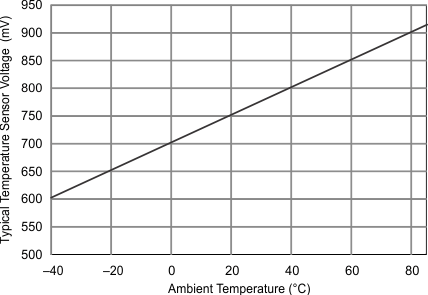 Figure 4-20 Typical Temperature Sensor Voltage
Table 4-33 lists the external reference requirements for the ADC.
Table 4-33 12-Bit ADC, External Reference(1)
over recommended ranges of supply voltage and operating free-air temperature (unless otherwise noted)| PARAMETER | TEST CONDITIONS | MIN | TYP | MAX | UNIT | |
|---|---|---|---|---|---|---|
| VR+ | Positive external reference voltage input VeREF+ or VeREF- based on ADC12VRSEL bit | VR+ > VR– | 1.2 | AVCC | V | |
| VR– | Negative external reference voltage input VeREF+ or VeREF- based on ADC12VRSEL bit | VR+ > VR– | 0 | 1.2 | V | |
| VR+ – VR– | Differential external reference voltage input | VR+ > VR– | 1.2 | AVCC | V | |
| IVeREF+, IVeREF- |
Static input current, singled-ended input mode | 1.2 V ≤ VeREF+ ≤ VAVCC, VeREF– = 0 V fADC12CLK = 5 MHz, ADC12SHTx = 1h, ADC12DIF = 0, ADC12PWRMD = 0 |
±10 | µA | ||
| 1.2 V ≤ VeREF+ ≤ VAVCC , VeREF– = 0 V fADC12CLK = 5 MHz, ADC12SHTx = 8h, ADC12DIF = 0, ADC12PWRMD = 01 |
±2.5 | |||||
| IVeREF+, IVeREF- |
Static input current, differential input mode | 1.2 V ≤ VeREF+ ≤ VAVCC, VeREF– = 0 V fADC12CLK = 5 MHz, ADC12SHTx = 1h, ADC12DIF = 1, ADC12PWRMD = 0 |
±20 | µA | ||
| 1.2 V ≤ VeREF+ ≤ VAVCC , VeREF– = 0 V fADC12CLK = 5 MHz, ADC12SHTx = 8h, ADC12DIF = 1, ADC12PWRMD = 1 |
±5 | |||||
| IVeREF+ | Peak input current with single-ended input | 0 V ≤ VeREF+ ≤ VAVCC, ADC12DIF = 0 | 1.5 | mA | ||
| IVeREF+ | Peak input current with differential input | 0 V ≤ VeREF+ ≤ VAVCC, ADC12DIF = 1 | 3 | mA | ||
| CVeREF+/- | Capacitance at VeREF+ or VeREF- terminal | See (2) | 10 | µF | ||
4.13.5.6 Reference
Table 4-34 lists the characteristics of the built-in voltage reference.
Table 4-34 REF, Built-In Reference
over recommended ranges of supply voltage and operating junction temperature (unless otherwise noted)| PARAMETER | TEST CONDITIONS | VCC | MIN | TYP | MAX | UNIT | |
|---|---|---|---|---|---|---|---|
| VREF+ | Positive built-in reference voltage output | REFVSEL = {2} for 2.5 V, REFON = 1 | 2.7 V | 2.5 | ±1.5% | V | |
| REFVSEL = {1} for 2.0 V, REFON = 1 | 2.2 V | 2.0 | ±1.5% | ||||
| REFVSEL = {0} for 1.2 V, REFON = 1 | 1.8 V | 1.2 | ±1.8% | ||||
| Noise | RMS noise at VREF(3) | From 0.1 Hz to 10 Hz, REFVSEL = {0} | 110 | µV | |||
| VOS_BUF_INT | VREF ADC BUF_INT buffer offset(4) | TJ = 25°C , ADC ON, REFVSEL = {0}, REFON = 1, REFOUT = 0 | –12 | +12 | mV | ||
| VOS_BUF_EXT | VREF ADC BUF_EXT buffer offset(4) | TJ = 25°C, REFVSEL = {0} , REFOUT = 1, REFON = 1 or ADC ON |
–12 | +12 | mV | ||
| AVCC(min) | AVCC minimum voltage, Positive built-in reference active | REFVSEL = {0} for 1.2 V | 1.8 | V | |||
| REFVSEL = {1} for 2.0 V | 2.2 | ||||||
| REFVSEL = {2} for 2.5 V | 2.7 | ||||||
| IREF+ | Operating supply current into AVCC terminal(1) | REFON = 1 | 3 V | 8 | 15 | µA | |
| IREF+_ADC_BUF | Operating supply current into AVCC terminal(1) | ADC ON, REFOUT = 0, REFVSEL = {0, 1, 2}, ADC12PWRMD = 0, | 3 V | 225 | 355 | µA | |
| ADC ON, REFOUT = 1, REFVSEL = {0, 1, 2}, ADC12PWRMD = 0 | 3 V | 1030 | 1660 | ||||
| ADC ON, REFOUT = 0, REFVSEL = {0, 1, 2}, ADC12PWRMD = 1 | 3 V | 120 | 185 | ||||
| ADC ON, REFOUT = 1, REFVSEL = {0, 1, 2}, ADC12PWRMD = 1 | 3 V | 545 | 895 | ||||
| ADC OFF, REFON = 1, REFOUT = 1, REFVSEL = {0, 1, 2} |
3 V | 1085 | |||||
| IO(VREF+) | VREF maximum load current, VREF+ terminal | REFVSEL = {0, 1, 2}, AVCC = AVCC(min) for each reference level, REFON = REFOUT = 1 |
–1000 | +10 | µA | ||
| ΔVout/ΔIo (VREF+) | Load-current regulation, VREF+ terminal | REFVSEL = {0, 1, 2}, IO(VREF+) = +10 µA or –1000 µA, AVCC = AVCC(min) for each reference level, REFON = REFOUT = 1 |
2500 | µV/mA | |||
| CVREF+/- | Capacitance at VREF+ and VREF- terminals | REFON = REFOUT = 1 | 0 | 100 | pF | ||
| TCREF+ | Temperature coefficient of built-in reference | REFVSEL = {0, 1, 2}, REFON = REFOUT = 1, TA = –55°C to 95°C(5) |
18 | 50 | ppm/K | ||
| PSRR_DC | Power supply rejection ratio (DC) | AVCC = AVCC(min) to AVCC(max), TJ = 25°C, REFVSEL = {0, 1, 2}, REFON = REFOUT = 1 |
120 | 400 | µV/V | ||
| PSRR_AC | Power supply rejection ratio (AC) | dAVCC= 0.1 V at 1 kHz | 3.0 | mV/V | |||
| tSETTLE | Settling time of reference voltage(2) | AVCC = AVCC (min) to AVCC(max), REFVSEL = {0, 1, 2}, REFON = 0 → 1 |
75 | 80 | µs | ||
4.13.5.7 Comparator
Table 4-35 lists the characteristics of the comparator.
Table 4-35 Comparator_E
over recommended ranges of supply voltage and operating junction temperature (unless otherwise noted)| PARAMETER | TEST CONDITIONS | VCC | MIN | TYP | MAX | UNIT | |
|---|---|---|---|---|---|---|---|
| IAVCC_COMP | Comparator operating supply current into AVCC, excludes reference resistor ladder | CEPWRMD = 00, CEON = 1, CERSx = 00 (fast) |
2.2 V, 3.0 V | 11 | 20 | µA | |
| CEPWRMD = 01, CEON = 1, CERSx = 00 (medium) |
9 | 17 | |||||
| CEPWRMD = 10, CEON = 1, CERSx = 00 (slow), TJ = 30°C |
0.6 | ||||||
| CEPWRMD = 10, CEON = 1, CERSx = 00 (slow), TJ = 95°C |
1.3 | ||||||
| IAVCC_REF | Quiescent current of resistor ladder into AVCC, including REF module current | CEREFLx = 01, CERSx = 10, REFON = 0, CEON = 0, CEREFACC = 0 |
2.2 V, 3.0 V | 12 | 15 | µA | |
| CEREFLx = 01, CERSx = 10, REFON = 0, CEON = 0, CEREFACC = 1 |
5 | 7 | |||||
| VREF | Reference voltage level | CERSx = 11, CEREFLx = 01, CEREFACC = 0 | 1.8 V | 1.17 | 1.2 | 1.23 | V |
| CERSx = 11, CEREFLx = 10, CEREFACC = 0 | 2.2 V | 1.92 | 2.0 | 2.08 | |||
| CERSx = 11, CEREFLx = 11, CEREFACC = 0 | 2.7 V | 2.40 | 2.5 | 2.60 | |||
| CERSx = 11, CEREFLx = 01, CEREFACC = 1 | 1.8 V | 1.10 | 1.2 | 1.245 | |||
| CERSx = 11, CEREFLx = 10, CEREFACC = 1 | 2.2 V | 1.90 | 2.0 | 2.08 | |||
| CERSx = 11, CEREFLx = 11, CEREFACC = 1 | 2.7 V | 2.35 | 2.5 | 2.60 | |||
| VIC | Common-mode input range | 0 | VCC-1 | V | |||
| VOFFSET | Input offset voltage | CEPWRMD = 00 | –32 | 32 | mV | ||
| CEPWRMD = 01 | –32 | 32 | |||||
| CEPWRMD = 10 | –30 | 30 | |||||
| CIN | Input capacitance | CEPWRMD = 00 or CEPWRMD = 01 | 9 | pF | |||
| CEPWRMD = 10 | 9 | ||||||
| RSIN | Series input resistance | On (switch closed) | 1 | 3 | kΩ | ||
| Off (switch open) | 50 | MΩ | |||||
| tPD | Propagation delay, response time | CEPWRMD = 00, CEF = 0, Overdrive ≥ 20 mV | 260 | 330 | ns | ||
| CEPWRMD = 01, CEF = 0, Overdrive ≥ 20 mV | 350 | 460 | |||||
| CEPWRMD = 10, CEF = 0, Overdrive ≥ 20 mV | 15 | µs | |||||
| tPD,filter | Propagation delay with filter active | CEPWRMD = 00 or 01, CEF = 1, Overdrive ≥ 20 mV, CEFDLY = 00 |
700 | 1000 | ns | ||
| CEPWRMD = 00 or 01, CEF = 1, Overdrive ≥ 20 mV, CEFDLY = 01 |
1.0 | 1.8 | µs | ||||
| CEPWRMD = 00 or 01, CEF = 1, Overdrive ≥ 20 mV, CEFDLY = 10 |
2.0 | 3.5 | |||||
| CEPWRMD = 00 or 01, CEF = 1, Overdrive ≥ 20 mV, CEFDLY = 11 |
4.0 | 7.0 | |||||
| tEN_CMP | Comparator enable time | CEON = 0 → 1, VIN+, VIN- from pins, Overdrive ≥ 20 mV, CEPWRMD = 00 |
0.9 | 1.5 | µs | ||
| CEON = 0 → 1, VIN+, VIN- from pins, Overdrive ≥ 20 mV, CEPWRMD = 01 |
0.9 | 1.5 | |||||
| CEON = 0 → 1, VIN+, VIN- from pins, Overdrive ≥ 20 mV, CEPWRMD = 10 |
15 | 100 | |||||
| tEN_CMP_VREF | Comparator and reference ladder and reference voltage enable time | CEON = 0 → 1, CEREFLX = 10, CERSx = 10 or 11, CEREF0 = CEREF1 = 0x0F, Overdrive ≥ 20 mV |
350 | 1500 | µs | ||
| VCE_REF | Reference voltage for a given tap | VIN = reference into resistor ladder, n = 0 to 31 |
VIN × (n + 0.5) / 32 | VIN × (n + 1) / 32 | VIN × (n + 1.5) / 32 | V | |
4.13.5.8 Scan Interface
Table 4-36 lists the port timing characteristics of the ESI.
Table 4-36 Extended Scan Interface, Port Drive, Port Timing
over recommended operating junction temperature range (unless otherwise noted)| PARAMETER | TEST CONDITIONS | VCC | MIN | TYP | MAX | UNIT | |
|---|---|---|---|---|---|---|---|
| VOL(ESICHx) | Voltage drop due to ON-resistance of excitation transistor (see Figure 4-21) | I(ESICHx) = 2 mA, ESITEN = 1 | 3 V | 0.3 | V | ||
| VOH(ESICHx) | Voltage drop due to ON-resistance of damping transistor(1) (see Figure 4-21) | I(ESICHx) = –200 µA, ESITEN = 1 | 3 V | 0.1 | V | ||
| VOL(ESICOM) | I(ESICOM) = 3 mA, ESISH = 1 | 2.2 V, 3 V | 0 | 0.1 | V | ||
| IESICHx(tri-state) | V(ESICHx) = 0 V to AVCC, port function disabled, ESISH = 1 |
3 V | –50 | 50 | nA | ||
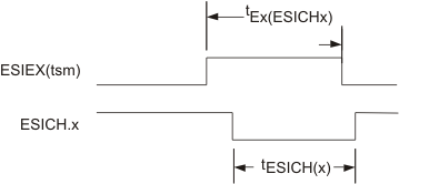 Figure 4-21 P6.x/ESICHx Timing, ESICHx Function Selected
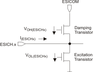 Figure 4-22 Voltage Drop Due to ON-Resistance
Table 4-37 lists the sample timing of the ESI.
Table 4-37 Extended Scan Interface, Sample Capacitor/Ri Timing (2)
over operating junction temperature range (unless otherwise noted)| PARAMETER | TEST CONDITIONS | VCC | MIN | TYP | MAX | UNIT | |
|---|---|---|---|---|---|---|---|
| CSHC(ESICHx) | Sample capacitance on selected ESICHx pin | ESIEx(tsm) = 1, ESISH = 1 | 2.2 V, 3 V | 7 | pF | ||
| Ri(ESICHx) | Serial input resistance at the ESICHx pin | ESIEx(tsm) = 1, ESISH = 1 | 2.2 V, 3 V | 1.5 | kΩ | ||
| tHold | Maximum hold time(1) | ESISHTSM(3) = 1, measurement sequence uses at least two ESICHx inputs, ΔVsample < 3 mV | 62 | µs | |||
Table 4-38 lists the characteristics of the ESI VCC/2 generator.
Table 4-38 Extended Scan Interface, VCC/2 Generator
over operating junction temperature range (unless otherwise noted)| PARAMETER | TEST CONDITIONS | VCC | MIN | TYP | MAX | UNIT | |
|---|---|---|---|---|---|---|---|
| VCC | ESI VCC/2 generator supply voltage | AVCC = DVCC = ESIDVCC (connected together), AVSS = DVSS = ESIDVSS (connected together) | 2.2 | 3.6 | V | ||
| IVMID | ESI VCC/2 generator quiescent current | CL at ESICOM pin = 470 nF ±20%, frefresh(ESICOM) = 32768 Hz, T = 0°C to 95°C, Rext = 1k in series to CL |
2.2 V, 3 V | 370 | 500 | nA | |
| CL at ESICOM pin = 470 nF ±20%, frefresh(ESICOM) = 32768 Hz, T = –55°C to 95°C |
370 | 1600 | |||||
| frefresh(ESICOM) | VCC/2 refresh frequency | Source clock = ACLK | 2.2 V, 3 V | 32.768 | kHz | ||
| V(ESICOM) | Output voltage at pin ESICOM | CL at ESICOM pin = 470 nF ±20%, ILoad = 1 µA |
AVCC / 2 –0.07 | AVCC / 2 | AVCC / 2 + 0.07 | V | |
| ton(ESICOM) | Time to reach 98% after VCC / 2 is switched on | CL at ESICOM pin = 470 nF ±20%, frefresh(ESICOM) = 32768 Hz |
2.2 V, 3 V | 1.7 | 6 | ms | |
| tVccSettle (ESICOM) | Settling time to ±VCC / 2560 (2 LSB) after AVCC voltage change | ESIEN = 1, ESIVMIDEN(1) = 1, ESISH = 0, AVCC = AVCC –100 mV, frefresh(ESICOM) = 32768 Hz |
2.2 V, 3 V | 3 | ms | ||
| AVCC = AVCC + 100 mV, frefresh(ESICOM) = 32768 Hz |
2.2 V, 3 V | 3 | |||||
Table 4-39 lists the characteristics of the ESI DAC.
Table 4-39 Extended Scan Interface, 12-Bit DAC
over operating junction temperature range (unless otherwise noted)| PARAMETER | TEST CONDITIONS | VCC | MIN | TYP | MAX | UNIT | |
|---|---|---|---|---|---|---|---|
| VCC | ESI DAC supply voltage | ESIDVCC = AVCC = DVCC (connected together), ESIDVSS = AVSS = DVSS (connected together) |
2.2 | 3.6 | V | ||
| ICC | ESI 12-bit DAC operating supply current into AVCC terminal (1) | 2.2 V | 10 | 27 | µA | ||
| 3 V | 14 | 35 | |||||
| Resolution | 12 | bit | |||||
| INL | Integral nonlinearity | RL = 1000 MΩ, CL = 20 pF With autozeroing |
2.2 V, 3 V | –10 | ±2 | +10 | LSB |
| DNL | Differential nonlinearity | RL = 1000 MΩ, CL = 20 pF, Without autozeroing |
2.2 V, 3 V | –10 | +10 | LSB | |
| RL = 1000 MΩ, CL = 20 pF, With autozeroing |
2.2 V, 3 V | –10 | +10 | LSB | |||
| EOS | Offset error | With autozeroing | 2.2 V, 3 V | 0 | V | ||
| EG | Gain error | With autozeroing | 2.2 V, 3 V | 0.6% | |||
| ton(ESIDAC) | On time after AVCC of ESIDAC is switched on | V+ESICA – VESIDAC = ±6 mV | 2.2 V, 3 V | 2 | µs | ||
| tSettle(ESIDAC) | Settling time | ESIDAC code = 0h → A0h | 2.2 V, 3 V | 2 | µs | ||
| ESIDAC code = A0h → 0h | 2.2 V, 3 V | 2 | |||||
Table 4-40 lists the characteristics of the ESI comparator.
Table 4-40 Extended Scan Interface, Comparator
over operating junction temperature range (unless otherwise noted)| PARAMETER | TEST CONDITIONS | VCC | MIN | TYP | MAX | UNIT | |
|---|---|---|---|---|---|---|---|
| VCC | ESI comparator supply voltage | ESIDVCC = AVCC = DVCC (connected together), ESIDVSS = AVSS = DVSS (connected together) |
2.2 | 3.6 | V | ||
| ICC | ESI comparator operating supply current into AVCC terminal (2) | 2.2 V, 3 V | 25 | 42 | µA | ||
| VIC | Common-mode input voltage range (1) | 2.2 V, 3 V | 0 | VCC – 1 | V | ||
| VOffset | Input offset voltage | After autozeroing | 2.2 V, 3 V | –1.5 | 1.5 | mV | |
| dVOffset/dT | Temperature coefficient of VOffset (3) | Without autozeroing | 2.2 V, 3 V | 40 | µV/°C | ||
| After autozeroing | 2 | ||||||
| dVOffset/dVCC | VOffset supply voltage (VCC) sensitivity(4) | Without autozeroing | 0.3 | mV/V | |||
| After autozeroing | 0.2 | ||||||
| Vhys | Input voltage hysteresis | V+ terminal = V- terminal = 0.5 × VCC | 2.2 V, 3 V | 0.5 | LSB | ||
| ton(ESICA) | On time after ESICA is switched on | V+ESICA – VESIDAC = +6 mV, V+ESICA = 0.5 × AVCC |
2.2 V, 3 V | 2.0 | µs | ||
| tSettle(ESICA) | Settle time | V+ESICA – VESIDAC = –12 mV → 6 mV, V+ESICA = 0.5 × AVCC |
2.2 V, 3 V | 3.0 | µs | ||
| tautozero | Autozeroing time of comparator | Vinput = VCC / 2, |Voffset| < 1 mV |
2.2 V, 3 V | 3.0 | µs | ||
Table 4-41 lists the characteristics of the ESI oscillator and clock.
Table 4-41 Extended Scan Interface, ESICLK Oscillator and TSM Clock Signals
over operating junction temperature range (unless otherwise noted)| PARAMETER | TEST CONDITIONS | VCC | MIN | TYP | MAX | UNIT | ||
|---|---|---|---|---|---|---|---|---|
| VCC | ESI oscillator supply voltage | ESIDVCC = AVCC = DVCC (connected together), ESIDVSS = AVSS = DVSS (connected together) |
2.2 | 3.6 | V | |||
| ICC | ESI oscillator operating supply current | fESIOSC= 4.8 MHz, ESIDIV1x = 00b, ESICLKGON = 1, ESIEN = 1, no TSM sequence running | 2.2 V | 45 | µA | |||
| 3 V | 50 | |||||||
| fESIOSC_min | ESI oscillator at minimum setting | TJ = 30°C, ESICLKFQ = 000000 | 2.3 | MHz | ||||
| fESIOSC_max | ESI oscillator at maximum setting | TJ = 30°C, ESICLKFQ = 111111 | 7.9 | MHz | ||||
| ton(ESIOSC) | Start-up time including synchronization cycles | fESIOSC = 4.8 MHz | 2.2 V, 3 V | 400 | ns | |||
| fESIOSC/dT | ESIOSC frequency temperature drift(1) | fESIOSC= 4.8 MHz | 2.2 V, 3 V | 0.15 | %/°C | |||
| fESIOSC/dVCC | ESIOSC frequency supply voltage drift (2) | fESIOSC= 4.8 MHz | 2.2 V, 3 V | 2 | %/V | |||
| fESILFCLK | TSM low-frequency state clock | 32.768 | 50 | kHz | ||||
| fESIHFCLK | TSM high-frequency state clock | 0.25 | 8 | MHz | ||||
4.13.5.9 FRAM Controller
Table 4-42 lists the characteristics of the FRAM.
Table 4-42 FRAM
over recommended ranges of supply voltage and operating junction temperature (unless otherwise noted)| PARAMETER | TEST CONDITIONS | MIN | TYP | MAX | UNIT | |
|---|---|---|---|---|---|---|
| Read and write endurance | 1015 | cycles | ||||
| tRetention | Data retention duration | TJ = 25°C | 100 | years | ||
| TJ = 70°C | 40 | |||||
| TJ = 95°C | 10 | |||||
| IWRITE | Current to write into FRAM | IREAD(1) | nA | |||
| IERASE | Erase current | n/a(2) | nA | |||
| tWRITE | Write time | tREAD(3) | ns | |||
| tREAD | Read time | NWAITSx = 0 | 1 / fSYSTEM(4) | ns | ||
| NWAITSx = 1 | 2 / fSYSTEM(4) | |||||
4.13.6 Emulation and Debug
Table 4-43 lists the characteristics of the JTAG and Spy-Bi-Wire interface.
Table 4-43 JTAG and Spy-Bi-Wire Interface
over recommended ranges of supply voltage and operating junction temperature (unless otherwise noted)| PARAMETER | TEST CONDITIONS | MIN | TYP | MAX | UNIT | |
|---|---|---|---|---|---|---|
| IJTAG | Supply current adder when JTAG active (but not clocked) | 2.2 V, 3.0 V | 40 | 100 | μA | |
| fSBW | Spy-Bi-Wire input frequency | 2.2 V, 3.0 V | 0 | 10 | MHz | |
| tSBW,Low | Spy-Bi-Wire low clock pulse duration | 2.2 V, 3.0 V | 0.04 | 15 | μs | |
| tSBW, En | Spy-Bi-Wire enable time (TEST high to acceptance of first clock edge)(1) | 2.2 V, 3.0 V | 110 | μs | ||
| tSBW,Rst | Spy-Bi-Wire return to normal operation time | 15 | 100 | μs | ||
| fTCK | TCK input frequency, 4-wire JTAG(2) | 2.2 V | 0 | 16 | MHz | |
| 3.0 V | 0 | 16 | MHz | |||
| Rinternal | Internal pulldown resistance on TEST | 2.2 V, 3.0 V | 20 | 35 | 50 | kΩ |
| fTCLK | TCLK/MCLK frequency during JTAG access, no FRAM access (limited by fSYSTEM) | 16 | MHz | |||
| tTCLK,Low/High | TCLK low or high clock pulse duration, no FRAM access |
25 | ns | |||
| fTCLK,FRAM | TCLK/MCLK frequency during JTAG access, including FRAM access (limited by fSYSTEM with no FRAM wait states) | 4 | MHz | |||
| tTCLK,FRAM,Low/High | TCLK low or high clock pulse duration, including FRAM accesses |
100 | ns | |||