JAJSGT8F June   2010  – March 2023 OPA140 , OPA2140 , OPA4140

PRODUCTION DATA  

  1.   1
  2. 特長
  3. アプリケーション
  4. 概要
  5. Revision History
  6. Pin Configuration and Functions
  7. Specifications
    1. 6.1 Absolute Maximum Ratings
    2. 6.2 ESD Ratings
    3. 6.3 Recommended Operating Conditions
    4. 6.4 Thermal Information: OPA140
    5. 6.5 Thermal Information: OPA2140
    6. 6.6 Thermal Information: OPA4140
    7. 6.7 Electrical Characteristics
    8. 6.8 Typical Characteristics
  8. Detailed Description
    1. 7.1 Overview
    2. 7.2 Functional Block Diagram
    3. 7.3 Feature Description
      1. 7.3.1  Operating Voltage
      2. 7.3.2  Capacitive Load and Stability
      3. 7.3.3  Output Current Limit
      4. 7.3.4  Noise Performance
      5. 7.3.5  Basic Noise Calculations
      6. 7.3.6  Phase-Reversal Protection
      7. 7.3.7  Thermal Protection
      8. 7.3.8  Electrical Overstress
      9. 7.3.9  EMI Rejection
      10. 7.3.10 EMIRR +IN Test Configuration
    4. 7.4 Device Functional Modes
  9. Application and Implementation
    1. 8.1 Application Information
    2. 8.2 Typical Application
      1. 8.2.1 Design Requirements
      2. 8.2.2 Detailed Design Procedure
      3. 8.2.3 Application Curve
    3. 8.3 Power Supply Recommendations
    4. 8.4 Layout
      1. 8.4.1 Layout Guidelines
      2. 8.4.2 Layout Example
  10. Device and Documentation Support
    1. 9.1 Device Support
      1. 9.1.1 Development Support
        1. 9.1.1.1 PSpice® for TI
        2. 9.1.1.2 TINA-TI™シミュレーション・ソフトウェア (無償ダウンロード)
        3. 9.1.1.3 フィルタ設計ツール
        4. 9.1.1.4 TI のリファレンス・デザイン
    2. 9.2 Documentation Support
      1. 9.2.1 Related Documentation
    3. 9.3 ドキュメントの更新通知を受け取る方法
    4. 9.4 サポート・リソース
    5. 9.5 Trademarks
    6. 9.6 静電気放電に関する注意事項
    7. 9.7 用語集
  11. 10Mechanical, Packaging, and Orderable Information

パッケージ・オプション

メカニカル・データ(パッケージ|ピン)
サーマルパッド・メカニカル・データ
発注情報

Detailed Design Procedure

The infinite-gain multiple-feedback circuit for a low-pass network function is shown in. Use Equation 2 to calculate the voltage transfer function.

Equation 2. GUID-1E140805-5FA5-4329-A030-A252744EB0F0-low.gif

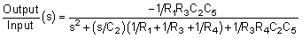
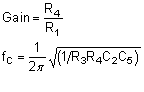
This circuit produces a signal inversion. For this circuit, the gain at DC and the low-pass cutoff frequency are calculated by Equation 3:

Equation 3. GUID-BB457378-78FB-4292-AA56-21A1DA713D2A-low.gif

Software tools are readily available to simplify filter design. The WEBENCH® Filter Designer is a simple, powerful, and easy-to-use active filter design program. The WEBENCH® Filter Designer lets you create optimized filter designs using a selection of TI operational amplifiers and passive components from TI's vendor partners.

Available as a web based tool from the WEBENCH Design Center, the WEBENCH Filter Designer allows you to design, optimize, and simulate complete, multistage, active-filter solutions within minutes.