SBOS484D December 2009 – April 2016 OPA1641 , OPA1642 , OPA1644
PRODUCTION DATA.
- 1 Features
- 2 Applications
- 3 Description
- 4 Revision History
- 5 Pin Configuration and Functions
- 6 Specifications
- 7 Detailed Description
- 8 Application and Implementation
- 9 Power Supply Recommendations
- 10Layout
- 11Device and Documentation Support
- 12Mechanical, Packaging, and Orderable Information
パッケージ・オプション
メカニカル・データ(パッケージ|ピン)
サーマルパッド・メカニカル・データ
発注情報
8 Application and Implementation
NOTE
Information in the following applications sections is not part of the TI component specification, and TI does not warrant its accuracy or completeness. TI’s customers are responsible for determining suitability of components for their purposes. Customers should validate and test their design implementation to confirm system functionality.
8.1 Application Information
The OPA1641, OPA1642, and OPA1644 are unity-gain stable, audio operational amplifiers with very low noise, input bias current, and input offset voltage. Applications with noisy or high-impedance power supplies require decoupling capacitors placed close to the device pins. In most cases, 0.1-μF capacitors are adequate. Figure 32 shows a simplified schematic of the OPA1641.
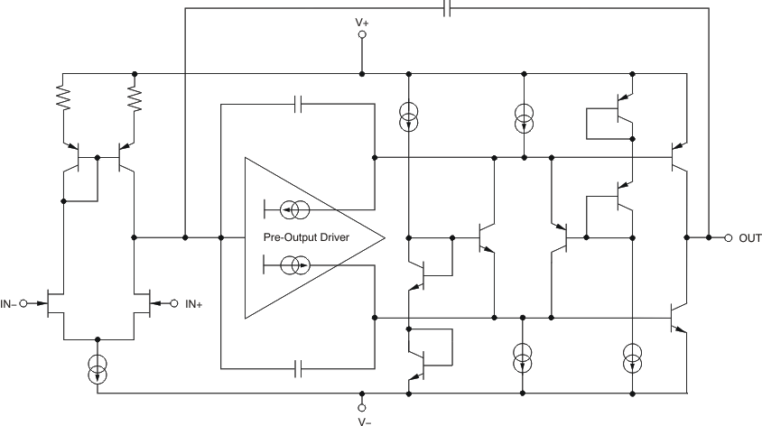 Figure 32. Simplified Internal Schematic
8.1.1 Noise Performance
Figure 33 illustrates the total circuit noise for varying source impedances with the operational amplifier in a unity-gain configuration (with no feedback resistor network and therefore no additional noise contributions). The OPA1641, OPA1642, and OPA1644 are shown with total circuit noise calculated. The operational amplifier contributes both a voltage noise component and a current noise component. The voltage noise is commonly modeled as a time-varying component of the offset voltage. The current noise is modeled as the time-varying component of the input bias current and reacts with the source resistance to create a voltage component of noise. Therefore, the lowest noise operational amplifier for a given application depends on the source impedance. For low source impedance, current noise is negligible, and voltage noise generally dominates. The OPA1641, OPA1642, and OPA1644 family has both low voltage noise and extremely low current noise because of the FET input of the operational amplifier. As a result, the current noise contribution of the OPA164x series is negligible for any practical source impedance, which makes the OPA164x series of amplifiers better choices for applications with high source impedance.
The equation in Figure 33 illustrates the calculation of the total circuit noise, where:
- en = voltage noise
- In = current noise
- RS = source impedance
- k = Boltzmann's constant = 1.38 × 10⁻²³ J/K
- T = temperature in degrees Kelvin (K)
For more details on calculating noise, see the Basic Noise Calculations section.
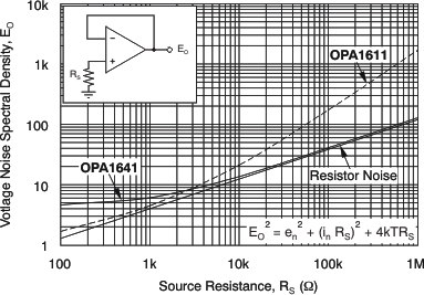 Figure 33. Noise Performance of the OPA1611 and OPA1641 in a Unity-Gain Buffer Configuration
8.1.2 Basic Noise Calculations
Low-noise circuit design requires careful analysis of all noise sources. External noise sources can dominate in many cases; consider the effect of source resistance on overall operational amplifier noise performance. Total noise of the circuit is the root-sum-square combination of all noise components.
The resistive portion of the source impedance produces thermal noise proportional to the square root of the resistance. This function is plotted in Figure 33. The source impedance is usually fixed; consequently, select the operational amplifier and the feedback resistors to minimize the respective contributions to the total noise.
Figure 34 illustrates both noninverting (A) and inverting (B) operational amplifier circuit configurations with gain. In circuit configurations with gain, the feedback network resistors also contribute noise. In general, the current noise of the operational amplifier reacts with the feedback resistors to create additional noise components. However, the extremely low current noise of the OPA164x means that the device current noise contribution can be neglected.
The feedback resistor values can generally be chosen to make these noise sources negligible. Note that low impedance feedback resistors do load the output of the amplifier. The equations for total noise are given in Figure 34 for both configurations.
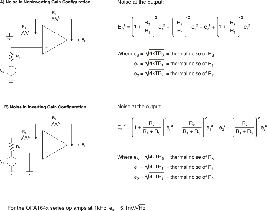 Figure 34. Noise Calculation in Gain Configurations
8.1.3 Total Harmonic Distortion Measurements
The OPA164x series operational amplifiers have excellent distortion characteristics. THD + noise is below 0.00005% (G = 1, VO = 3 VRMS, BW = 80 kHz) throughout the audio frequency range, 20 Hz to 20 kHz, with a
2-kΩ load (see Figure 7).
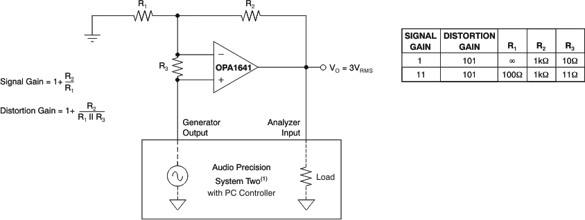
The distortion produced by the OPA164x series operational amplifiers is below the measurement limit of many commercially available distortion analyzers. However, a special test circuit (such as shown in Figure 35) can be used to extend the measurement capabilities.
Operational amplifier distortion can be considered an internal error source that can be referred to the input. Figure 35 shows a circuit that causes the operational amplifier distortion to be 101 times (or approximately 40 dB) greater than that normally produced by the operational amplifier. The addition of R3 to the otherwise standard noninverting amplifier configuration alters the feedback factor or noise gain of the circuit. The closed-loop gain is unchanged, but the feedback available for error correction is reduced by a factor of 101, thus extending the resolution by 101. Note that the input signal and load applied to the operational amplifier are the same as with conventional feedback without R3. Keep the value of R3 small to minimize any effect on distortion measurements.
The validity of this technique can be verified by duplicating measurements at high gain or high frequency where the distortion is within the measurement capability of the test equipment. Measurements for this document were made with an audio precision system two distortion and noise analyzer that greatly simplifies such repetitive measurements. The measurement technique can, however, be performed with manual distortion measurement instruments.
space
8.1.4 Source Impedance and Distortion
In traditional JFET-input operational amplifiers, the impedance applied to the positive and negative inputs in noninverting applications must be matched for lowest distortion. Legacy methods for fabricating the JFETs in the FET input stage exhibit a varying input capacitance with applied common-mode input voltage. In inverting configurations, the input does not vary with input voltage because the inverting input is held at virtual ground. However, in noninverting applications, the inputs do vary, and the gate-to-source voltage is not constant. This effect produces increased distortion as a result of the varying capacitance for unmatched source impedances. However, the OPA164x family of amplifiers is designed to maintain a constant input capacitance with varying common-mode voltage to prevent this mechanism of distortion. The variation of input capacitance with common-mode voltage for a traditional amplifier is compared to the OPA164x family in Figure 36.
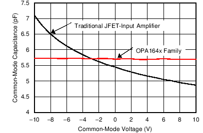 Figure 36. Input Capacitance of the OPA164x Family of Amplifiers Compared to Traditional JFET-input Amplifiers
By stabilizing the input capacitance, the distortion performance of the amplifier is greatly improved for noninverting configurations with high source impedances. The measured performance of an OPA164x amplifier is compared to a traditional JFET-input amplifier in Figure 37. The unity-gain configuration, high source impedance, and large-signal amplitude produce additional distortion in the traditional amplifier.
 Figure 37. Measured THD+N of the OPA164x Family of Amplifiers Compared to Traditional JFET-input Amplifiers
8.1.5 Capacitive Load and Stability
The dynamic characteristics of the OPA164x are optimized for commonly encountered gains, loads, and operating conditions. The combination of low closed-loop gain and high capacitive loads decreases the phase margin of the amplifier and can lead to gain peaking or oscillations. As a result, heavier capacitive loads must be isolated from the output. The simplest way to achieve this isolation is to add a small resistor (ROUT equal to 50 Ω, for example) in series with the output.
Figure 19 and Figure 20 illustrate graphs of Small-Signal Overshoot vs Capacitive Load for several values of ROUT. Also, see Applications Bulletin AB-028, Feedback Plots Define Op Amp AC Performance (SBOA015) available for download at www.ti.com for details of analysis techniques and application circuits.
8.1.6 Power Dissipation and Thermal Protection
The OPA164x series of operational amplifiers are capable of driving 2-kΩ loads with power-supply voltages of up to ±18 V over the specified temperature range. In a single-supply configuration, where the load is connected to the negative supply voltage, the minimum load resistance is 2.8 kΩ at a supply voltage of 36 V. For lower supply voltages (either single-supply or symmetrical supplies), a lower load resistance can be used, as long as the output current does not exceed 13 mA; otherwise, the device short-circuit current protection circuit can activate.
Internal power dissipation increases when operating at high supply voltages. Copper leadframe construction used in the OPA1641, OPA1642, and OPA1644 series of devices improves heat dissipation compared to conventional materials. PCB layout can also help reduce a possible increase in junction temperature. Wide copper traces help dissipate the heat by functioning as an additional heatsink. Temperature rise can be further minimized by soldering the devices directly to the PCB rather than using a socket.
Although the output current is limited by internal protection circuitry, accidental shorting one or more output channels of a device can result in excessive heating. For instance, when an output is shorted to mid-supply, the typical short-circuit current of 36 mA leads to an internal power dissipation of over 600 mW at a supply of ±18 V. In case of a dual OPA1642 in an VSSOP-8 package (thermal resistance θJA = 180°C/W), such a power dissipation results in the die temperature to be 220°C above ambient temperature, when both channels are shorted. This temperature increase will destroy the device.
To prevent such excessive heating that can destroy the device, the OPA164x series has an internal thermal shutdown circuit that shuts down the device if the die temperature exceeds approximately 180°C. When this thermal shutdown circuit activates, a built-in hysteresis of 15°C ensures that the die temperature must drop to approximately 165°C before the device switches on again.
8.1.7 Electrical Overstress
Designers often ask questions about the capability of an operational amplifier to withstand electrical overstress. These questions tend to focus on the device inputs, but can involve the supply voltage pins or even the output pin. Each of these different pin functions have electrical stress limits determined by the voltage breakdown characteristics of the particular semiconductor fabrication process and specific circuits connected to the pin. Additionally, internal electrostatic discharge (ESD) protection is built into these circuits to protect them from accidental ESD events both before and during product assembly.
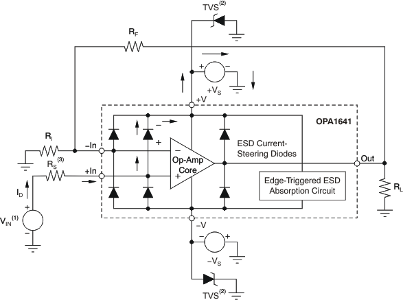
Having a good understanding of this basic ESD circuitry and its relevance to an electrical overstress event is helpful. Figure 38 illustrates the ESD circuits contained in the OPA164x series (indicated by the dashed line area). The ESD protection circuitry involves several current-steering diodes connected from the input and output pins and routed back to the internal power-supply lines where an internal absorption device is connected. This protection circuitry is intended to remain inactive during normal circuit operation.
An ESD event produces a short duration, high-voltage pulse that is transformed into a short-duration, high-current pulse when discharging through a semiconductor device. The ESD protection circuits are designed to provide a current path around the operational amplifier core to prevent damage. The energy absorbed by the protection circuitry is then dissipated as heat.
When an ESD voltage develops across two or more of the amplifier device pins, current flows through one or more of the steering diodes. Depending on the path that the current takes, the absorption device can activate. The absorption device has a trigger, or threshold voltage, that is above the normal operating voltage of the OPA164x but below the device breakdown voltage level. When this threshold is exceeded, the absorption device quickly activates and clamps the voltage across the supply rails to a safe level.
When the operational amplifier connects into a circuit such as the one illustrated in Figure 38, the ESD protection components are intended to remain inactive and not become involved in the application circuit operation. However, circumstances can arise where an applied voltage exceeds the operating voltage range of a given pin. If this condition occurs, some of the internal ESD protection circuits can be biased on and conduct current. Any such current flow occurs through steering diode paths and rarely involves the absorption device.
Figure 38 depicts a specific example where the input voltage, VIN, exceeds the positive supply voltage (+VS) by 500 mV or more. Much of what happens in the circuit depends on the supply characteristics. If +VS can sink the current, one of the upper input steering diodes conducts and directs current to +VS. Excessively high current levels can flow with increasingly higher VIN. As a result, the datasheet specifications recommend that applications limit the input current to 10 mA.
If the supply is not capable of sinking the current, VIN can begin sourcing current to the operational amplifier, and then take over as the source of positive supply voltage. The danger in this case is that the voltage can rise to levels that exceed the operational amplifier absolute maximum ratings.
Another common question involves what happens to the amplifier if an input signal is applied to the input when the power supplies +VS and –VS are at 0 V. The amplifier behavior depends on the supply characteristic when at 0 V, or at a level below the input signal amplitude. If the supplies appear as high impedance, then the operational amplifier supply current can be supplied by the input source through the current steering diodes. This state is not a normal bias condition; the amplifier most likely will not operate normally. If the supplies are low impedance, then the current through the steering diodes can become quite high. The current level depends on the ability of the input source to deliver current, and any resistance in the input path.
If there is an uncertainty about the ability of the supply to absorb this current, external Zener diodes can be added to the supply pins, as shown in Figure 38. The Zener voltage must be selected such that the diode does not turn on during normal operation. However, the Zener voltage must be low enough so that the Zener diode conducts if the supply pin begins to rise above the safe operating supply voltage level.
8.2 Typical Application
The noise and distortion performance of the OPA164x family of amplifiers is exceptional in applications with high source impedances, which makes these devices an excellent choice in preamplifier circuits for moving magnet phono cartridges. The high source impedance of the cartridge, and high gain required by the RIAA playback curve at low frequency, requires an amplifier with both low input current noise and low input voltage noise.
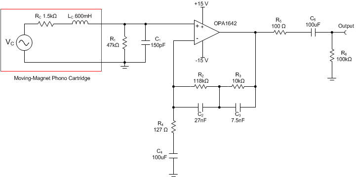 Figure 39. Preamplifier Circuit for Vinyl Record Playback With Moving-Magnet Phono Cartridges
 (Single Channel Shown)
8.2.1 Design Requirements
- Gain: 40 dB (1 kHz)
- RIAA Accuracy: ±0.5 dB (100 Hz to 20 kHz)
- Power Supplies: ±15 V
8.2.2 Detailed Design Procedure
Vinyl records are recorded using an equalization curve specified by the Recording Institute Association of America (RIAA). The purpose of this equalization curve is to decrease the amount of space occupied by a grove on the record and therefore maximize the amount of information able to be stored. Proper playback of music stored on the record requires a preamplifier circuit that applies the inverse transfer function of the recording equalization curve. The combination of the recording equalization and the playback equalization results in a flat frequency response over the audio range; see Figure 40.
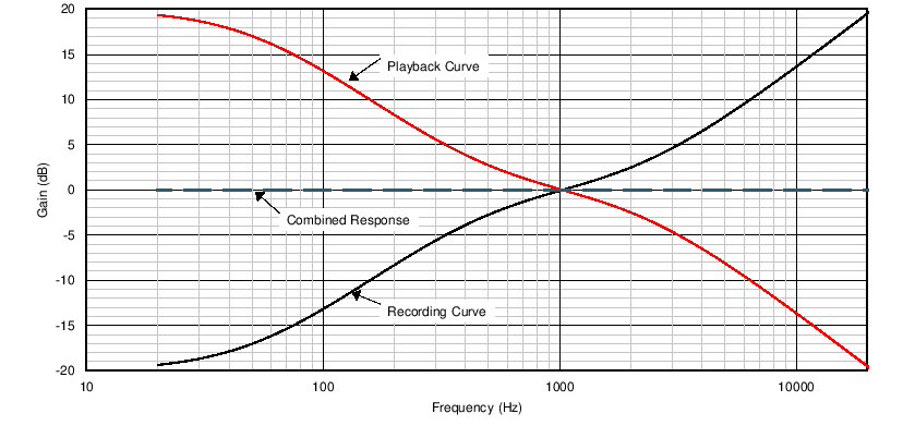 Figure 40. RIAA Recording and Playback Curves Normalized at 1 kHz
The basic RIAA playback curve implements three time constants: 75 μs, 380 μs, and 3180 μs. An IEC amendment is later added to the playback curve and implements a pole in the curve at 20 Hz with the intent of protecting loudspeakers from excessive low frequency content. Rather than strictly adhering to the IEC amendment, this design moves this pole to a lower frequency to improve low frequency response and still providing protection for loudspeakers.
Resistor R1 and capacitor C1 are selected to provide the proper input impedance for the moving magnet cartridge. Cartridge loading is specified by the manufacturer in the cartridge datasheet and is absolutely crucial for proper response at high frequency. 47 kΩ is a common value for the input resistor, and the capacitive loading is usually specified to 200 pF to 300 pF per channel. This capacitive loading specification includes the capacitance of the cable connecting the turntable to the preamplifier, as well as any additional parasitic capacitances at the preamplifier input. Therefore, the value of C1 must be less than the loading specification to account for these additional capacitances.
The output network consisting of R5, R6, and C5 serves to ac couple the preamplifier circuit to any subsequent electronics in the signal path. The 100-Ω resistor R5 limits in-rush current into coupling capacitor C5 and prevents parasitic capacitance from cabling from causing instability. R6 prevents charge accumulation on C5. Capacitor C5 is chosen to be the same value as C4; for simplicity however, the value of C5 must be large enough to avoid attenuating low frequency information.
The feedback resistor elements must be selected to provide the correct response within the audio bandwidth. In order to achieve the correct frequency response, the passive components in Figure 39 must satisfy Equation 1, Equation 2, and Equation 3:


R2, R3, and R4 must also be selected to meet the design requirements for gain. The gain at 1 kHz is determined by subtracting 20 dB from gain of the circuit at very low frequency (near dc), as shown in Equation 4:

Therefore, the low frequency gain of the circuit must be 60 dB to meet the goal of 40 dB at 1 kHz and is determined by resistors R2, R3, and R4 as shown in Equation 5:

Because there are multiple combinations of passive components that satisfy these equations, a spreadsheet or other software calculation tool is the easiest method to examine resistor and capacitor combinations.
Capacitor C4 forces the gain of the circuit to unity at dc in order to limit the offset voltage at the output of the preamplifier circuit. The high-pass corner frequency created by this capacitor is calculated by Equation 6:

The circuit described in Figure 39 is constructed with 1% tolerance resistors and 5% tolerance NP0, C0G ceramic capacitors without any additional hand sorting. The large value of C4 typically requires an electrolytic type to be used. However, electrolytic capacitors have the potential to introduce distortion into the signal path. This circuit is constructed using a bipolar electrolytic capacitor specifically intended for audio applications.
8.2.3 Application Curves
The deviation from the ideal RIAA transfer function curve is shown in Figure 41 and normalized to an ideal gain of 40 dB at 1 kHz. The measured gain at 1 kHz is 0.05 dB less than the design goal, and the maximum deviation from 100 Hz to 20 kHz is 0.18 dB. The deviation from the ideal curve can be improved by hand-sorting resistor and capacitor values to their ideal values. The value of C4 can also be increased to reduce the deviation at low frequency.
A spectrum of the preamplifier output signal is shown in Figure 42 for a 10 mVRMS, 1-kHz input signal (1-VRMS output). All distortion harmonics are below the preamplifier noise floor.
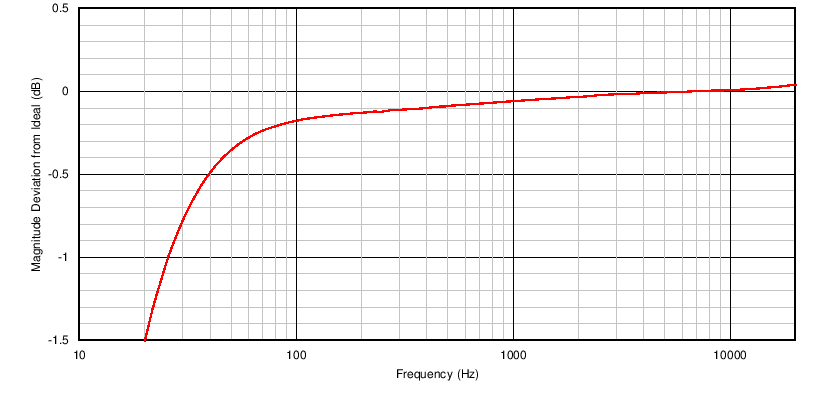 Figure 41. Measured Deviation from Ideal RIAA Response
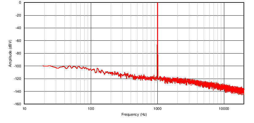 Figure 42. Output Spectrum for a 10 mVRMS, 1 kHz Input Signal
