SLOS805C July 2012 – August 2016 OPA1662-Q1
PRODUCTION DATA.
- 1 Features
- 2 Applications
- 3 Description
- 4 Revision History
- 5 Description Continued
- 6 Pin Configuration and Functions
- 7 Specifications
- 8 Detailed Description
- 9 Application and Implementation
- 10Power Supply Recommendations
- 11Layout
- 12Device and Documentation Support
- 13Mechanical, Packaging, and Orderable Information
パッケージ・オプション
メカニカル・データ(パッケージ|ピン)
サーマルパッド・メカニカル・データ
発注情報
11 Layout
11.1 Layout Guidelines
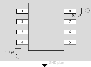
The OPA1662-Q1 is a unity-gain stable, precision dual op amp with very low noise. To realize the full operational performance of the device, good high-frequency printed-circuit board (PCB) layout practices are required. Low-loss, 0.1-µF bypass capacitors must be connected between each supply pin and ground as close to the device as possible. The bypass capacitor traces must be designed for minimum inductance.
11.2 Layout Example
 Figure 52. Layout Recommendation
11.3 Power Dissipation
The OPA1662-Q1 op amp is capable of driving 2-kΩ loads with a power-supply voltage up to ±18 V and full operating temperature range. Internal power dissipation increases when operating at high supply voltages. Copper leadframe construction used in the OPA1662-Q1 op amp improves heat dissipation compared to conventional materials. Circuit board layout can also help minimize junction temperature rise. Wide copper traces help dissipate the heat by acting as an additional heat sink. Temperature rise can be further minimized by soldering the devices to the circuit board rather than using a socket.