JAJSGG7B January   2019  – August 2019 OPA1671

PRODUCTION DATA.  

  1. 特長
  2. アプリケーション
  3. 概要
    1.     Device Images
      1.      エレクトレット・マイク・プリアンプ
      2.      OPA1671の電圧ノイズ密度
  4. 改訂履歴
  5. Pin Configuration and Functions
    1.     Pin Functions
  6. Specifications
    1. 6.1 Absolute Maximum Ratings
    2. 6.2 ESD Ratings
    3. 6.3 Recommended Operating Conditions
    4. 6.4 Thermal Information
    5. 6.5 Electrical Characteristics
    6. 6.6 Typical Characteristics
  7. Detailed Description
    1. 7.1 Overview
    2. 7.2 Functional Block Diagram
    3. 7.3 Feature Description
      1. 7.3.1 Operating Voltage
      2. 7.3.2 Input Bias Current
      3. 7.3.3 Common-Mode Voltage Range
      4. 7.3.4 EMI Susceptibility and Input Filtering
    4. 7.4 Device Functional Modes
  8. Application and Implementation
    1. 8.1 Application Information
      1. 8.1.1 Capacitive Loads
      2. 8.1.2 Noise Performance
      3. 8.1.3 Basic Noise Calculations
    2. 8.2 Typical Application
      1. 8.2.1 Design Requirements
      2. 8.2.2 Detailed Design Procedure
      3. 8.2.3 Application Curves
  9. Power Supply Recommendations
  10. 10Layout
    1. 10.1 Layout Guidelines
    2. 10.2 Layout Example
  11. 11デバイスおよびドキュメントのサポート
    1. 11.1 デバイス・サポート
      1. 11.1.1 開発サポート
        1. 11.1.1.1 TINA-TI(無料のダウンロード・ソフトウェア)
    2. 11.2 ドキュメントのサポート
      1. 11.2.1 関連資料
    3. 11.3 ドキュメントの更新通知を受け取る方法
    4. 11.4 コミュニティ・リソース
    5. 11.5 商標
    6. 11.6 静電気放電に関する注意事項
    7. 11.7 Glossary
  12. 12メカニカル、パッケージ、および注文情報

パッケージ・オプション

メカニカル・データ(パッケージ|ピン)
サーマルパッド・メカニカル・データ
発注情報

Input Bias Current

Typically, input bias current is approximately ±10 pA. Input voltages exceeding the power supplies, however, can cause excessive current to flow into or out of the input pins. Momentary voltages greater than the power supply can be tolerated if the input current is limited to 10 mA. This limitation is easily accomplished with an input resistor, as shown in Figure 30.

Unlike many operational amplifiers, there are no diodes connected between the positive and negative input terminals. As a result, differential voltages up to the full supply voltage do not cause any significantly higher current flow into the inputs.
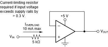
OPA1671 OPA1671_Input_Current_Limit.gifFigure 30. Input Current Protection