JAJSOU7A September 2015 – June 2022 OPA1688
PRODUCTION DATA
- 1 特長
- 2 アプリケーション
- 3 概要
- 4 Revision History
- 5 Device Comparison Table
- 6 Pin Configuration and Functions
- 7 Specifications
- 8 Detailed Description
- 9 Applications and Implementation
- 10Power Supply Recommendations
- 11Layout
- 12Device and Documentation Support
- 13Mechanical, Packaging, and Orderable Information
パッケージ・オプション
メカニカル・データ(パッケージ|ピン)
サーマルパッド・メカニカル・データ
- DRG|8
発注情報
9.2.1.2 Detailed Design Procedure
The OPA1688 offers an excellent combination of specifications for headphone amplifier circuits (such as low noise, low distortion, capacitive load stability, and relatively high output current). Furthermore, the low-power supply current and small package options make the OPA1688 an excellent choice for headphone amplifiers in portable devices. A common headphone amplifier circuit for audio digital-to-analog converters (DACs) with differential voltage outputs is illustrated in Figure 9-1. This circuit converts the differential voltage output of the DAC to a single-ended, ground-referenced signal and provides the additional current necessary for low-impedance headphones. For R2 = R4 and R1 = R3, the output voltage of the circuit is given by Equation 1:
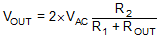
where
- ROUT is the output impedance of the DAC
- 2 × VAC is the unloaded differential output voltage
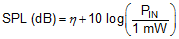
The output voltage required for headphones depends on the headphone impedance as well as the headphone efficiency. Both values can be provided by the headphone manufacturer, with headphone efficiency usually given as a sound pressure level (SPL) produced with 1 mW of input power and denoted by the Greek letter η. The SPL at other input power levels can be calculated from the efficiency specification using Equation 2:
At extremely high power levels, the accuracy of this calculation decreases as a result of secondary effects in the headphone drivers. Figure 9-2 allows the SPL produced by a pair of headphones of a known sensitivity to be estimated for a given input power.
 Figure 9-2 SPLs Produced for Various Headphone Efficiencies and Input Power Levels
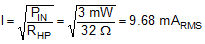
For example, a pair of headphones with a 95-dB/mW sensitivity given a 3-mW input signal produces a 100-dB SPL. If these headphones have a nominal impedance of 32 Ω, then Equation 3 and Equation 4 describe the voltage and current from the headphone amplifier, respectively:

Headphones can present a capacitive load at high frequencies that can destabilize the headphone amplifier circuit. Many headphone amplifiers use a resistor in series with the output to maintain stability; however this solution also compromises audio quality. The OPA1688 is able to maintain stability into large capacitive loads; therefore, a series output resistor is not necessary in the headphone amplifier circuit. TINA-TI™ simulations illustrate that the circuit in Figure 9-1 has a phase margin of approximately 50° with a 400-pF load connected directly to the amplifier output.