JAJSE79C June 2017 – October 2018 OPA1692
PRODUCTION DATA.
- 1 特長
- 2 アプリケーション
- 3 概要
- 4 改訂履歴
- 5 Pin Configuration and Functions
- 6 Specifications
- 7 Detailed Description
- 8 Application and Implementation
- 9 Power Supply Recommendations
- 10Layout
- 11デバイスおよびドキュメントのサポート
- 12メカニカル、パッケージ、および注文情報
パッケージ・オプション
メカニカル・データ(パッケージ|ピン)
サーマルパッド・メカニカル・データ
- DGK|8
発注情報
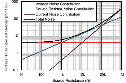
8.1.2 Noise Performance
Figure 56 shows the total circuit noise for varying source impedances with the operational amplifier in a unity-gain configuration (with no feedback resistor network and therefore no additional noise contributions). The op amp itself contributes a voltage noise component and a current noise component. The voltage noise is commonly modeled as a time-varying component of the offset voltage. The current noise is modeled as the time-varying component of the input bias current and reacts with the source resistance to create a voltage component of noise. Therefore, the lowest noise op amp for a given application depends on the source impedance. For low source impedance, current noise is negligible, and voltage noise generally dominates. The OPA169x has low voltage noise and low current noise. As a result, the current noise contribution of the OPA169x series is negligible for source impedances less than 100 kΩ.
Figure 56 shows the calculation of the total circuit noise, with these parameters:
- en = voltage noise
- In = current noise
- RS = source impedance
- k = Boltzmann's constant = 1.38 × 10⁻²³ J/K
- T = temperature in degrees Kelvin (K)
For more details on calculating noise, see Basic Noise Calculations.
 Figure 56. Noise Performance of the OPA169x in a Unity-Gain Buffer Configuration