JAJSCP9 December 2016 OPA2836-Q1
PRODUCTION DATA.
- 1 特長
- 2 アプリケーション
- 3 概要
- 4 改訂履歴
- 5 OPA2836-Q1 Related Devices
- 6 Pin Configuration and Functions
- 7 Specifications
- 8 Detailed Description
-
9 Application and Implementation
- 9.1
Application Information
- 9.1.1 Noninverting Amplifier
- 9.1.2 Inverting Amplifier
- 9.1.3 Instrumentation Amplifier
- 9.1.4 Attenuators
- 9.1.5 Single-Ended-to-Differential Amplifier
- 9.1.6 Differential-to-Signal-Ended Amplifier
- 9.1.7 Differential-to-Differential Amplifier
- 9.1.8 Pulse Application With Single-Supply
- 9.1.9 ADC Driver Performance
- 9.2 Typical Applications
- 9.1
Application Information
- 10Power Supply Recommendations
- 11Layout
- 12デバイスおよびドキュメントのサポート
- 13メカニカル、パッケージ、および注文情報
11 Layout
11.1 Layout Guidelines
The OPA835DBV, OPA836DBV EVM (SLOU314) must be used as a reference when designing the circuit board. Follow the EVM layout of the external components near to the amplifier, ground plane construction, and power routing as closely as possible. General guidelines are:
- Signal routing must be direct and as short as possible into an out of the operational amplifier.
- The feedback path must be short and direct avoiding vias if possible especially with G = +1.
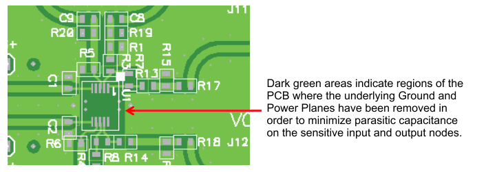
- Ground or power planes must be removed from directly under the negative input and output pins of the amplifier.
- A series output resistor is recommended to be placed as near to the output pin as possible. See Figure 17 for recommended values given expected capacitive load of design.
- A 2.2-µF power-supply decoupling capacitor must be placed within 2 inches of the device and can be shared with other operational amplifiers. For spit supply, a capacitor is required for both supplies.
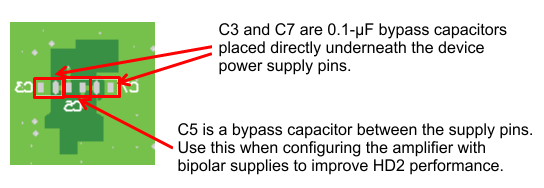
- A 0.1-µF power-supply decoupling capacitor must be placed as near to the power supply pins as possible. Preferably within 0.1 inch. For split supply, a capacitor is required for both supplies.
11.2 Layout Example
 Figure 78. Top Layer
 Figure 79. Bottom Layer