SBOS513F August 2010 – December 2016 OPA2320 , OPA320
PRODUCTION DATA.
- 1 Features
- 2 Applications
- 3 Description
- 4 Revision History
- 5 Pin Configuration and Functions
- 6 Specifications
-
7 Detailed Description
- 7.1 Overview
- 7.2 Functional Block Diagram
- 7.3
Feature Description
- 7.3.1 Operating Voltage
- 7.3.2 Input and ESD Protection
- 7.3.3 Rail-to-Rail Input
- 7.3.4 Phase Reversal
- 7.3.5 Feedback Capacitor Improves Response
- 7.3.6 EMI Susceptibility and Input Filtering
- 7.3.7 Output Impedance
- 7.3.8 Capacitive Load and Stability
- 7.3.9 Overload Recovery Time
- 7.3.10 Shutdown Function
- 7.3.11 Leadless SON Package
- 7.4 Device Functional Modes
- 8 Application and Implementation
- 9 Power Supply Recommendations
- 10Layout
- 11Device and Documentation Support
- 12Mechanical, Packaging, and Orderable Information
パッケージ・オプション
メカニカル・データ(パッケージ|ピン)
サーマルパッド・メカニカル・データ
発注情報
7 Detailed Description
7.1 Overview
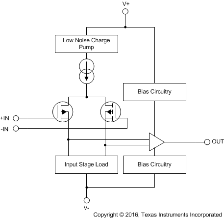
The OPA320 family of operational amplifiers (op amps) are high-speed, precision amplifiers, perfectly suited to drive 12-, 14-, and 16-bit analog-to-digital converters. Low output impedance with flat frequency characteristics and zero-crossover distortion circuitry enable high linearity over the full input common mode range, achieving true rail-to-rail input from a 1.8-V to 5.5-V single supply.
7.2 Functional Block Diagram
7.3 Feature Description
7.3.1 Operating Voltage
The OPA320 series op amps are unity-gain stable and can operate on a single-supply voltage (1.8 V to 5.5 V), or a split-supply voltage (±0.9 V to ±2.75 V), making them highly versatile and easy to use. The power-supply pins should have local bypass ceramic capacitors (typically 0.001 µF to 0.1 µF). The OPA320 amplifiers are fully specified from 1.8 V to 5.5 V and over the extended temperature range of –40°C to 125°C. Parameters that can exhibit variance with regard to operating voltage or temperature are presented in the Typical Characteristics.
7.3.2 Input and ESD Protection
The OPA320 incorporates internal electrostatic discharge (ESD) protection circuits on all pins. In the case of input and output pins, this protection primarily consists of current-steering diodes connected between the input and power-supply pins. These ESD protection diodes also provide in-circuit input overdrive protection, provided that the current is limited to 10 mA as stated in the Absolute Maximum Ratings. Many input signals are inherently current-limited to less than 10 mA; therefore, a limiting resistor is not required. Figure 33 shows how a series input resistor (RS) may be added to the driven input to limit the input current. The added resistor contributes thermal noise at the amplifier input and the value should be kept to the minimum in noise-sensitive applications.
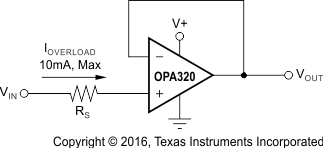 Figure 33. Input Current Protection
7.3.3 Rail-to-Rail Input
The OPA320 product family features true rail-to-rail input operation, with supply voltages as low as ±0.9 V (1.8 V). The design of the OPA320 amplifiers include an internal charge-pump that powers the amplifier input stage with an internal supply rail at approximately 1.6 V above the external supply (VS+). This internal supply rail allows the single differential input pair to operate and remain very linear over a very wide input common mode range. A unique zero-crossover input topology eliminates the input offset transition region typical of many rail-to-rail, complementary input stage operational amplifiers. This topology allows the OPA320 to provide superior common-mode performance (CMRR > 110 dB, typical) over the entire common-mode input range, which extends 100 mV beyond both power-supply rails. When driving analog-to-digital converters (ADCs), the highly linear VCM range of the OPA320 assures maximum linearity and lowest distortion.
7.3.4 Phase Reversal
The OPA320 op amps are designed to be immune to phase reversal when the input pins exceed the supply voltages, therefore providing further in-system stability and predictability. Figure 34 shows the input voltage exceeding the supply voltage without any phase reversal.
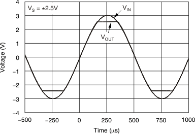 Figure 34. No Phase Reversal
7.3.5 Feedback Capacitor Improves Response
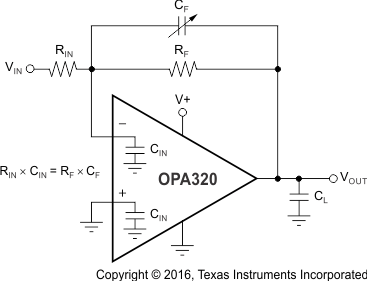
For optimum settling time and stability with high-impedance feedback networks, it may be necessary to add a feedback capacitor across the feedback resistor, RF, as shown in Figure 35. This capacitor compensates for the zero created by the feedback network impedance and the OPA320 input capacitance (and any parasitic layout capacitance). The effect becomes more significant with higher impedance networks.
NOINDENT:
Where CIN is equal to the OPA320 input capacitance (approximately 9 pF) plus any parasitic layout capacitance.For the circuit shown in Figure 35, the value of the variable feedback capacitor should be chosen so that the input resistance times the input capacitance of the OPA320 (typically 9 pF) plus the estimated parasitic layout capacitance equals the feedback capacitor times the feedback resistor calculated with Equation 1.
where
- CIN is equal to the OPA320 input capacitance (sum of differential and common mode) plus the layout capacitance.
The capacitor value can be adjusted until optimum performance is obtained.
7.3.6 EMI Susceptibility and Input Filtering
Operational amplifiers vary in susceptibility to electromagnetic interference (EMI). If conducted EMI enters the operational amplifier, the dc offset observed at the amplifier output may shift from the nominal value while EMI is present. This shift is a result of signal rectification associated with the internal semiconductor junctions. While all operational amplifier pin functions can be affected by EMI, the input pins are likely to be the most susceptible. The OPA320 operational amplifier family incorporates an internal input low-pass filter that reduces the amplifiers response to EMI. Both common mode and differential mode filtering are provided by the input filter. The filter is designed for a cutoff frequency of approximately 580 MHz (–3 dB), with a roll-off of 20 dB per decade.
7.3.7 Output Impedance
The open-loop output impedance of the OPA320 common-source output stage is approximately 90 Ω. When the op amp is connected with feedback, this value is reduced significantly by the loop gain. For example, with 130 dB (typical) of open-loop gain, the output impedance is reduced in unity-gain to less than 0.03 Ω. For each decade rise in the closed-loop gain, the loop gain is reduced by the same amount, which results in a ten-fold increase in effective output impedance. While the OPA320 output impedance remains very flat over a wide frequency range, at higher frequencies the output impedance rises as the open-loop gain of the op amp drops. However, at these frequencies the output also becomes capacitive as a result of parasitic capacitance. This architecture in turn prevents the output impedance from becoming too high, which can cause stability problems when driving large capacitive loads. As mentioned previously, the OPA320 has excellent capacitive load drive capability for an op amp with its bandwidth.
7.3.8 Capacitive Load and Stability
The OPA320 is designed to be used in applications where driving a capacitive load is required. As with all op amps, there may be specific instances where the OPA320 can become unstable. The particular op amp circuit configuration, layout, gain, and output loading are some of the factors to consider when establishing whether an amplifier is stable in operation. An op amp in the unity-gain (1-V/V) buffer configuration and driving a capacitive load exhibits a greater tendency to become unstable than an amplifier operated at a higher noise gain. The capacitive load, in conjunction with the op amp output resistance, creates a pole within the feedback loop that degrades the phase margin. The degradation of the phase margin increases as the capacitive loading increases. When operating in the unity-gain configuration, the OPA320 remains stable with a pure capacitive load up to approximately 1 nF.
The equivalent series resistance (ESR) of some very large capacitors (CL > 1 µF) is sufficient to alter the phase characteristics in the feedback loop such that the amplifier remains stable. Increasing the amplifier closed-loop gain allows the amplifier to drive increasingly larger capacitance. This increased capability is evident when observing the overshoot response of the amplifier at higher voltage gains, as shown in Figure 37. One technique for increasing the capacitive load drive capability of the amplifier operating in unity gain is to insert a small resistor (RS), typically 10 Ω to 20 Ω, in series with the output, as shown in Figure 36.
This resistor significantly reduces the overshoot and ringing associated with large capacitive loads. A possible problem with this technique is that a voltage divider is created with the added series resistor and any resistor connected in parallel with the capacitive load. The voltage divider introduces a gain error at the output that reduces the output swing. The error contributed by the voltage divider may be insignificant. For instance, with a load resistance, RL = 10 kΩ and RS = 20 Ω, the gain error is only about 0.2%. However, when RL is decreased to 600 Ω, which the OPA320 is able to drive, the error increases to 7.5%.
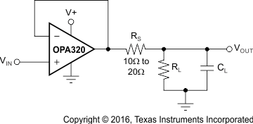 Figure 36. Improving Capacitive Load Drive
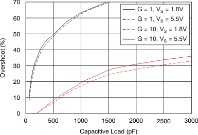 Figure 37. Small-Signal Overshoot vs Capacitive Load (100-mVPP Output Step)
7.3.9 Overload Recovery Time
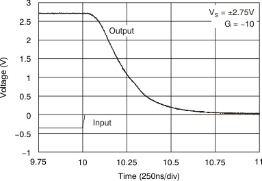
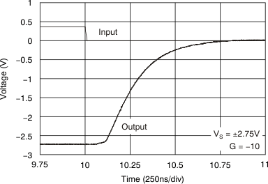
Overload recovery time is the time it takes the output of the amplifier to come out of saturation and recover to the linear region. Overload recovery is particularly important in applications where small signals must be amplified in the presence of large transients. Figure 38 and Figure 39 show the positive and negative overload recovery times of the OPA320, respectively. In both cases, the time elapsed before the OPA320 comes out of saturation is less than 100 ns. In addition, the symmetry between the positive and negative recovery times allows excellent signal rectification without distortion of the output signal.
7.3.10 Shutdown Function
The SHDN (enable) pin function of the OPAx320S is referenced to the negative supply voltage of the operational amplifier. A logic level high enables the op amp. A valid logic high is defined as voltage [(V+) – 0.1 V], up to (V+), applied to the SHDN pin. A valid logic low is defined as [(V–) + 0.1 V], down to (V–), applied to the enable pin. The maximum allowed voltage applied to SHDN is 5.5 V with respect to the negative supply, independent of the positive supply voltage. This pin must either be connected to a valid high or a low voltage or driven, and not left as an open circuit.
The logic input is a high-impedance CMOS input. Dual op amp versions are independently controlled and quad op amp versions are controlled in pairs with logic inputs. For battery-operated applications, this feature may be used to greatly reduce the average current and extend battery life. The enable time is 10 µs for full shutdown of all channels; disable time is 3 μs. When disabled, the output assumes a high-impedance state. This architecture allows the OPAx320S to be operated as a gated amplifier (or to have the device output multiplexed onto a common analog output bus). Shutdown time (tOFF) depends on loading conditions and increases with increased load resistance. To ensure shutdown (disable) within a specific shutdown time, the specified 10-kΩ load to mid-supply (VS / 2) is required. If using the OPAx320S without a load, the resulting turn-off time is significantly increased.
7.3.11 Leadless SON Package
The OPA320 series uses the SON style package (also known as SON), which is a QFN with contacts on only two sides of the package bottom. This leadless package maximizes printed circuit board (PCB) space and offers enhanced thermal and electrical characteristics through an exposed pad. One of the primary advantages of the SON package is its low height (0.8 mm).
SON packages are physically small, have a smaller routing area, improved thermal performance, reduced electrical parasitics, and a pinout scheme that is consistent with other commonly-used packages (such as SOIC and VSSOP). Additionally, the absence of external leads eliminates bent-lead issues.
The SON package can easily be mounted using standard PCB assembly techniques. See Application Report, QFN/SON PCB Attachment (SLUA271) and Application Report, Quad Flatpack No-Lead Logic Packages (SCBA017), both available for download at www.ti.com.
NOTE
The exposed leadframe die pad on the bottom of the SON package should be connected to the most negative potential (V–).
7.4 Device Functional Modes
The OPA320 family of operational amplifiers are operational when power-supply voltages between 1.8 V to 5.5 V are applied. Devices with an S suffix have a shutdown capability. For a detailed description of the shutdown function, see Shutdown Function.
