JAJS010E March 2006 – December 2015 OPA2333 , OPA333
PRODUCTION DATA.
- 1 特長
- 2 アプリケーション
- 3 概要
- 4 改訂履歴
- 5 Pin Configuration and Functions
- 6 Specifications
- 7 Detailed Description
- 8 Application and Implementation
- 9 Power Supply Recommendations
- 10Layout
- 11デバイスおよびドキュメントのサポート
- 12メカニカル、パッケージ、および注文情報
パッケージ・オプション
メカニカル・データ(パッケージ|ピン)
サーマルパッド・メカニカル・データ
発注情報
10 Layout
10.1 Layout Guidelines
10.1.1 General Layout Guidelines
Pay attention to good layout practices. Keep traces short and when possible, use a printed-circuit-board (PCB) ground plane with surface-mount components placed as close to the device pins as possible. Place a 0.1-μF capacitor closely across the supply pins. Apply these guidelines throughout the analog circuit to improve performance and provide benefits, such as reducing the electromagnetic interference (EMI) susceptibility.
Operational amplifiers vary in susceptibility to radio frequency interference (RFI). RFI can generally be identified as a variation in offset voltage or DC signal levels with changes in the interfering RF signal. The OPA333 is specifically designed to minimize susceptibility to RFI and demonstrates remarkably low sensitivity compared to previous generation devices. Strong RF fields may still cause varying offset levels.
10.1.2 DFN Layout Guidelines
Solder the exposed leadframe die pad on the DFN package to a thermal pad on the PCB. A mechanical drawing showing an example layout is attached at the end of this data sheet. Refinements to this layout may be necessary based on assembly process requirements. Mechanical drawings located at the end of this data sheet list the physical dimensions for the package and pad. The five holes in the landing pattern are optional, and are intended for use with thermal vias that connect the leadframe die pad to the heatsink area on the PCB.
Soldering the exposed pad significantly improves board-level reliability during temperature cycling, key push, package shear, and similar board-level tests. Even with applications that have low-power dissipation, the exposed pad must be soldered to the PCB to provide structural integrity and long-term reliability.
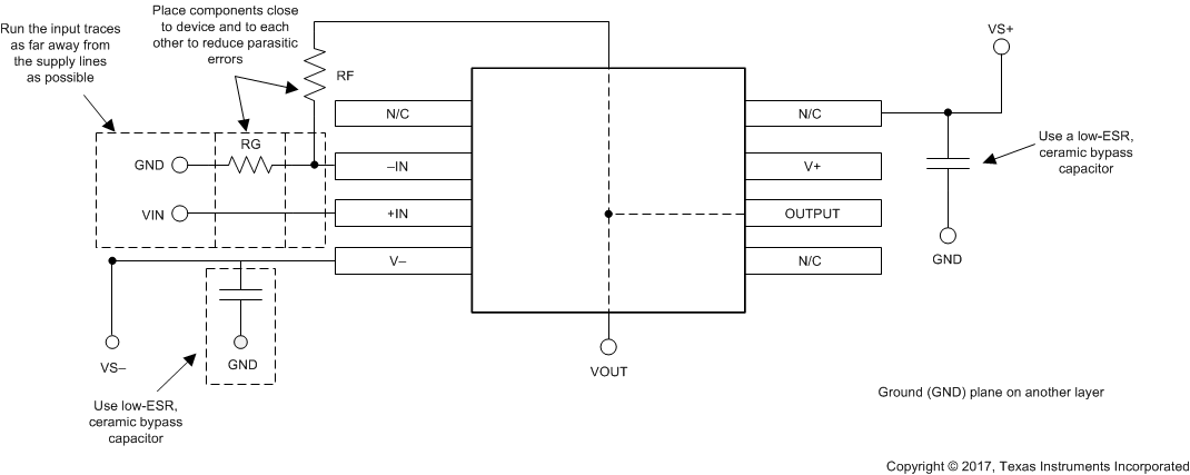
10.2 Layout Example
 Figure 34. Layout Example