SBOS099D September 2000 – December 2015 OPA2350 , OPA350 , OPA4350
PRODUCTION DATA.
- 1 Features
- 2 Applications
- 3 Description
- 4 Revision History
- 5 Pin Configuration and Functions
- 6 Specifications
- 7 Detailed Description
-
8 Application and Implementation
- 8.1 Application Information
- 8.2 Typical Applications
- 9 Power Supply Recommendations
- 10Layout
- 11Device and Documentation Support
- 12Mechanical, Packaging, and Orderable Information
パッケージ・オプション
メカニカル・データ(パッケージ|ピン)
サーマルパッド・メカニカル・データ
発注情報
7 Detailed Description
7.1 Overview
The OPA350 series rail-to-rail CMOS operational amplifiers are optimized for low voltage, single-supply operation. Rail-to-rail input and output, low noise (5 nV/√Hz), and high speed operation (38 MHz, 22 V/μs) make the amplifiers ideal for driving sampling Analog-to-Digital (A/D) converters. They are also suited for cell phone PA control loops and video processing (75-Ω drive capability), as well as audio and general purpose applications. Single, dual, and quad versions have identical specifications for maximum design flexibility.
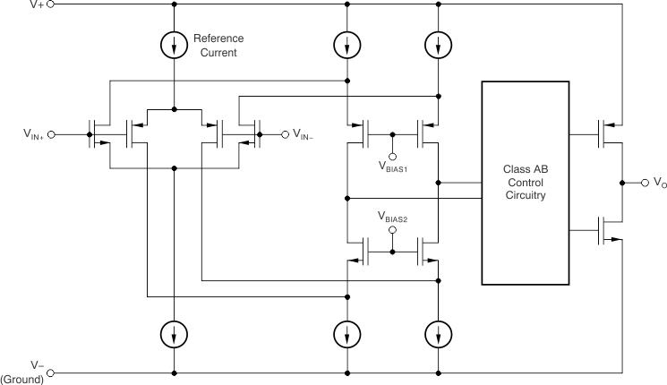
7.2 Functional Block Diagram
7.3 Feature Description
The OPA350 series of operational amplifiers (op amps) are fabricated on a state-of-the-art 0.6 micron CMOS process. They are unity-gain stable and suitable for a wide range of general purpose applications. Rail-to-rail input and output make them ideal for driving sampling A/D converters. They are also suited for controlling the output power in cell phones. These applications often require high speed and low noise. In addition, the OPA350 series offers a low-cost solution for general-purpose and consumer video applications (75-Ω drive capability).
Excellent AC performance makes the OPA350 series suited for audio applications. Their bandwidth, slew rate, low noise (5 nV/√Hz), low THD (0.0006%), and small package options are ideal for these applications. The class AB output stage is capable of driving 600-Ω loads connected to any point between V+ and ground.
Rail-to-rail input and output swing significantly increases dynamic range, especially in low voltage supply applications. Figure 25 shows the input and output waveforms for the OPA350 in unity-gain configuration. Operation is from a single 5-V supply with a 1-kΩ load connected to VS/2. The input is a 5 VPP sinusoid. Output voltage swing is approximately 4.95 VPP.
Power supply pins should be bypassed with 0.01-μF ceramic capacitors.
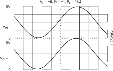 Figure 25. Rail-to-Rail Input and Output
7.3.1 Operating Voltage
OPA350 series operational amplifiers are fully specified from 2.7 V to 5.5 V. Supply voltage may range from 2.5 V to 5.5 V. Parameters are tested over the specified supply range: a feature of the OPA350 series. In addition, many specifications apply from −40°C to 85°C. Most behavior remains virtually unchanged throughout the full operating voltage range. Parameters that vary significantly with operating voltage or temperature are shown in Typical Characteristics.
7.3.2 Rail-to-Rail Input
The tested input common-mode voltage range of the OPA350 series extends 100 mV beyond the supply rails. This is achieved with a complementary input stage: an N-channel input-differential pair in parallel with a P-channel differential pair, as shown in Figure 26. The N-channel pair is active for input voltages close to the positive rail, typically (V+) – 1.8 V to 100 mV above the positive supply, while the P-channel pair is on for inputs from 100 mV below the negative supply to approximately (V+) – 1.8 V. There is a small transition region, typically (V+) – 2 V to (V+) – 1.6 V, in which both pairs are on. This 400-mV transition region can vary ±400 mV with process variation. Thus, the transition region (both input stages on) can range from (V+) – 2.4 V to (V+) – 2 V on the low end, up to (V+) – 1.6 V to (V+) – 1.2 V on the high end.
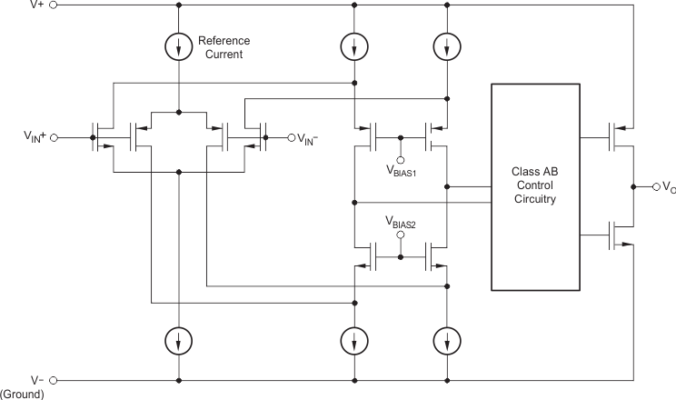 Figure 26. Simplified Schematic
OPA350 series operational amplifiers are laser-trimmed to reduce offset voltage difference between the N-channel and P-channel input stages, resulting in improved common-mode rejection and a smooth transition between the N-channel pair and the P-channel pair. However, within the 400-mV transition region PSRR, CMRR, offset voltage, offset drift, and THD may be degraded compared to operation outside this region.
A double-folded cascode adds the signal from the two input pairs and presents a differential signal to the class AB output stage. Normally, input bias current is approximately 500 fA. However, large inputs (greater than 300 mV beyond the supply rails) can turn on the input protection diodes, causing excessive current to flow in or out of the input pins. Momentary voltages greater than 300 mV beyond the power supply can be tolerated if the current on the input pins is limited to 10 mA. This is easily accomplished with an input resistor, as shown in Figure 27. Many input signals are inherently current-limited to less than 10 mA; therefore, a limiting resistor is not required.
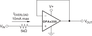 Figure 27. Input Current Protection for Voltages Exceeding the Supply Voltage
7.3.3 Rail-to-Rail Output
A class AB output stage with common-source transistors achieves rail-to-rail output. For light resistive loads (>10 kΩ), the output voltage swing is typically ten millivolts from the supply rails. With heavier resistive loads (600 Ω to 10 kΩ), the output can swing to within a few tens of millivolts from the supply rails and maintain high open-loop gain. See Figure 17 and Figure 18 for more information.
7.3.4 Capacitive Load and Stability
OPA350 series operational amplifiers can drive a wide range of capacitive loads. However, all operational amplifiers under certain conditions may become unstable. operational amplifier configuration, gain, and load value are just a few of the factors to consider when determining stability. An operational amplifier in unity-gain configuration is the most susceptible to the effects of capacitive load. The capacitive load reacts with the output impedance of the operational amplifier, along with any additional load resistance, to create a pole in the small-signal response that degrades the phase margin.
In unity gain, OPA350 series operational amplifiers perform well with large capacitive loads. Increasing gain enhances the ability of the amplifier to drive more capacitance. Figure 21 shows performance with a 1-kΩ resistive load. Increasing load resistance improves capacitive load drive capability.
7.3.5 Driving A/D Converters
OPA350 series operational amplifiers are optimized for driving medium speed (up to 500 kHz) sampling A/D converters, and also offer excellent performance for higher speed converters. The OPA350 series provides an effective means of buffering the input capacitance of the A/D and resulting charge injection while providing signal gain.
Figure 28 shows the OPA350 driving an ADS7861. The ADS7861 is a dual, 500 kHz, 12-bit sampling converter in the tiny SSOP-24 package. When used with the miniature package options of the OPA350 series, the combination is ideal for space-limited applications. For further information, consult the ADS7861 data sheet, Dual, 500kSPS, 12-Bit, 2 + 2 Channel, Simultaneous Sampling ANALOG-TO-DIGITAL CONVERTER (SBAS110).
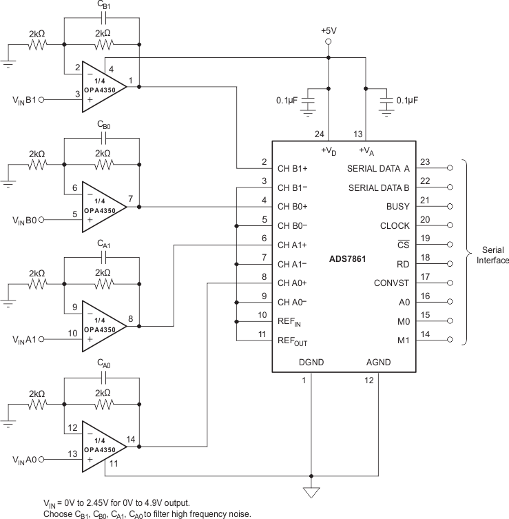 Figure 28. OPA4350 Driving Sampling A/D Converter
7.3.6 Output Impedance
The low-frequency open-loop output impedance of the common-source output stage of the OPA350 is approximately 1 kΩ. When the operational amplifier is connected with feedback, this value is reduced significantly by the loop gain of the operational amplifier. For example, with 122 dB of open-loop gain, the output impedance is reduced in unity-gain to less than 0.001 Ω. For each decade rise in the closed-loop gain, the loop gain is reduced by the same amount which results in a ten-fold increase in effective output impedance (see Figure 15).
At higher frequencies, the output impedance rises as the open-loop gain of the operational amplifier drops. However, at these frequencies the output also becomes capacitive due to parasitic capacitance. This prevents the output impedance from becoming too high, which can cause stability problems when driving capacitive loads. The OPA350 has excellent capacitive load drive capability for an operational amplifier with its bandwidth.
7.4 Device Functional Modes
The OPAx350 has a single functional mode and is operational when the power-supply voltage is greater than
2.7 V (±1.35 V). The maximum power supply voltage for the OPAx350 is 5.5V (±2.75 V).