JAJSEY7C January 2016 – March 2018 OPA197 , OPA2197 , OPA4197
PRODUCTION DATA.
- 1 特長
- 2 アプリケーション
- 3 概要
- 4 改訂履歴
- 5 Pin Configuration and Functions
-
6 Specifications
- 6.1 Absolute Maximum Ratings
- 6.2 ESD Ratings
- 6.3 Recommended Operating Conditions
- 6.4 Thermal Information: OPA197
- 6.5 Thermal Information: OPA2197
- 6.6 Thermal Information: OPA4197
- 6.7 Electrical Characteristics: VS = ±4 V to ±18 V (VS = 8 V to 36 V)
- 6.8 Electrical Characteristics: VS = ±2.25 V to ±4 V (VS = 4.5 V to 8 V)
- 6.9 Typical Characteristics
- 7 Detailed Description
- 8 Application and Implementation
- 9 Power Supply Recommendations
- 10Layout
- 11デバイスおよびドキュメントのサポート
- 12メカニカル、パッケージ、および注文情報
パッケージ・オプション
メカニカル・データ(パッケージ|ピン)
サーマルパッド・メカニカル・データ
- D|14
発注情報
7.3.1 Input Protection Circuitry
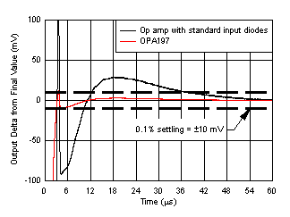
The OPAx197 uses a unique input architecture to eliminate the need for input protection diodes, but still provides robust input protection under transient conditions. Conventional input diode protection schemes shown in Figure 41 can be activated by fast transient step responses and can introduce signal distortion and settling time delays because of alternate current paths, as shown in Figure 42. For low-gain circuits, these fast-ramping input signals forward-bias back-to-back diodes, causing an increase in input current, and resulting in extended settling time, as shown in Figure 43.
 Figure 41. OPA197 Input Protection Does Not Limit Differential Input Capability
 Figure 42. Back-to-Back Diodes Create Settling Issues
 Figure 43. OPA197 Protection Circuit Maintains Fast-Settling Transient Response
The OPAx197 family of operational amplifiers provides a true high-impedance differential input capability for high-voltage applications. This patented input protection architecture does not introduce additional signal distortion or delayed settling time, making the device an optimal op amp for multichannel, high-switched, input applications. The OPA197 can tolerate a maximum differential swing (voltage between inverting and noninverting pins of the op amp) of up to 36 V, making the device suitable for use as a comparator or in applications with fast-ramping input signals such as multiplexed data-acquisition systems, as shown in Figure 53.