JAJSOU8B June   2022  – November 2022 OPA4991-EP

PRODUCTION DATA  

  1. 特長
  2. アプリケーション
  3. 概要
  4. Revision History
  5. Pin Configuration and Functions
  6. Specifications
    1. 6.1 Absolute Maximum Ratings
    2. 6.2 ESD Ratings
    3. 6.3 Recommended Operating Conditions
    4. 6.4 クワッド・チャネルの熱に関する情報
    5. 6.5 Electrical Characteristics
    6. 6.6 Typical Characteristics
  7. Detailed Description
    1. 7.1 Overview
    2. 7.2 Functional Block Diagram
    3. 7.3 Feature Description
      1. 7.3.1 Input Protection Circuitry
      2. 7.3.2 EMI Rejection
      3. 7.3.3 Thermal Protection
      4. 7.3.4 Capacitive Load and Stability
      5. 7.3.5 Common-Mode Voltage Range
      6. 7.3.6 Phase Reversal Protection
      7. 7.3.7 Electrical Overstress
      8. 7.3.8 Overload Recovery
      9. 7.3.9 Typical Specifications and Distributions
    4. 7.4 Device Functional Modes
  8. Application and Implementation
    1. 8.1 Application Information
    2. 8.2 Typical Applications
      1. 8.2.1 Low-Side Current Measurement
        1. 8.2.1.1 Design Requirements
        2. 8.2.1.2 Detailed Design Procedure
        3. 8.2.1.3 Application Curve
    3. 8.3 Power Supply Recommendations
    4. 8.4 Layout
      1. 8.4.1 Layout Guidelines
      2. 8.4.2 Layout Example
  9. Device and Documentation Support
    1. 9.1 Device Support
      1. 9.1.1 Development Support
        1. 9.1.1.1 TINA-TI (Free Software Download)
    2. 9.2 Documentation Support
      1. 9.2.1 Related Documentation
    3. 9.3 Receiving Notification of Documentation Updates
    4. 9.4 サポート・リソース
    5. 9.5 Trademarks
    6. 9.6 Electrostatic Discharge Caution
    7. 9.7 Glossary
  10. 10Mechanical, Packaging, and Orderable Information

パッケージ・オプション

メカニカル・データ(パッケージ|ピン)
サーマルパッド・メカニカル・データ
発注情報

Detailed Design Procedure

The transfer function of the circuit in Figure 8-1 is given in Equation 1.

Equation 1. GUID-197A5AAE-6F3B-4AF9-9688-7B38CADD7C6D-low.gif

The load current (ILOAD) produces a voltage drop across the shunt resistor (RSHUNT). The load current is set from 0 A to 1 A. To keep the shunt voltage below 100 mV at maximum load current, the largest shunt resistor is defined using Equation 2.

Equation 2. GUID-8D821B22-7D85-4174-8013-7F07A5F983AD-low.gif

Using Equation 2, RSHUNT is calculated to be 100 mΩ. The voltage drop produced by ILOAD and RSHUNT is amplified by the OPA4991-EP to produce an output voltage of 0 V to 4.9 V. The gain needed by the OPA4991-EP to produce the necessary output voltage is calculated using Equation 3.

Equation 3. GUID-B9571D2E-6856-4F1D-BB47-E2C628FAC79C-low.gif

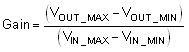
Using Equation 3, the required gain is calculated to be 49 V/V, which is set with resistors RF and RG. Equation 4 is used to size the resistors, RF and RG, to set the gain of the OPA4991-EP to 49 V/V.

Equation 4. GUID-28817D8D-3C45-4A36-9813-B6BAE4F7D651-low.gif

Choosing RF as 360 kΩ, RG is calculated to be 7.5 kΩ. RF and RG were chosen as 360 kΩ and 7.5 kΩ because they are standard value resistors that create a 49:1 ratio. Other resistors that create a 49:1 ratio can also be used. Figure 8-2 shows the measured transfer function of the circuit shown in Figure 8-1.