SBOS342C December 2008 – November 2015 OPA659
PRODUCTION DATA.
- 1 Features
- 2 Applications
- 3 Description
- 4 Revision History
- 5 Related Operational Amplifier Products
- 6 Pin Configuration and Functions
- 7 Specifications
- 8 Detailed Description
- 9 Application Information
- 10Power Supply Recommendations
- 11Layout
- 12Device and Documentation Support
- 13Mechanical, Packaging, and Orderable Information
パッケージ・オプション
メカニカル・データ(パッケージ|ピン)
サーマルパッド・メカニカル・データ
- DRB|8
発注情報
9 Application Information
NOTE
Information in the following applications sections is not part of the TI component specification, and TI does not warrant its accuracy or completeness. TI’s customers are responsible for determining suitability of components for their purposes. Customers should validate and test their design implementation to confirm system functionality.
9.1 Application Information
9.1.1 Wideband, Noninverting Operation
The OPA659 is a very broadband, unity-gain stable, voltage-feedback amplifier with a high impedance JFET-input stage. Its very high gain bandwidth product (GBP) of 350 MHz can be used to either deliver high signal bandwidths for low-gain buffers, or to deliver broadband, low-noise, transimpedance bandwidth to photodiode-detector applications. The OPA659 is designed to provide very low distortion and accurate pulse response with low overshoot and ringing. To achieve the full performance of the OPA659, careful attention to printed-circuit board (PCB) layout and component selection are required, as discussed in the remaining sections of this data sheet.
Figure 35 shows the noninverting gain of +1 circuit; Figure 36 shows the more general circuit used for other noninverting gains. These circuits are used as the basis for most of the noninverting gain Typical Characteristics graphs. Most of the graphs were characterized using signal sources with 50-Ω driving impedance, and with measurement equipment presenting a 50-Ω load impedance. In Figure 35, the shunt resistor RT at VIN should be set to 50 Ω to match the source impedance of the test generator and cable, while the series output resistor, ROUT, at VOUT should also be set to 50 Ω to provide matching impedance for the measurement equipment load and cable. Generally, data sheet voltage swing specifications are measured at the output pin, VOUT, in Figure 35 and Figure 36.
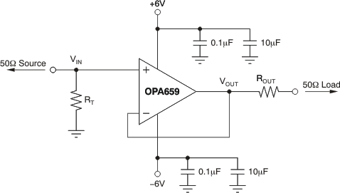 Figure 35. Noninverting Gain of +1 Test Circuit
Voltage-feedback op amps can use a wide range of resistor values to set the gain. To retain a controlled frequency response for the noninverting voltage amplifier of Figure 36, the parallel combination of RF || RG should always be less than 200 Ω. In the noninverting configuration, the parallel combination of
RF || RG forms a pole with the parasitic input and board layout capacitance at the inverting input of the OPA659. For best performance, this pole should be at a frequency greater than the closed-loop bandwidth for the OPA659. For this reason, TI recommends a direct short from the output to the inverting input for the unity-gain follower application. Table 2 lists several recommended resistor values for noninverting gains with a 50-Ω input and output match.
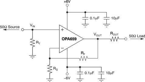 Figure 36. General Noninverting Test Circuit
Table 2. Resistor Values for Noninverting Gains With 50-Ω Input/Output Match
| NONINVERTING GAIN | RF | RG | RT | ROUT |
|---|---|---|---|---|
| +1 | 0 | Open | 49.9 | 49.9 |
| +2 | 249 | 249 | 49.9 | 49.9 |
| +5 | 249 | 61.9 | 49.9 | 49.9 |
| +10 | 249 | 27.4 | 49.9 | 49.9 |
9.1.2 Wideband, Inverting Gain Operation
The circuit of Figure 37 shows the inverting gain test circuit used for most of the inverting Typical Characteristics graphs. As with the noninverting applications, most of the curves were characterized using signal sources with 50-Ω driving impedance, and with measurement equipment that presents a 50-Ω load impedance. In Figure 37, the shunt resistor RT at VIN should be set so the parallel combination of the shunt resistor and RG equals 50 Ω to match the source impedance of the test generator and cable, while the series output resistor ROUT at VOUT should also be set to 50 Ω to provide matching impedance for the measurement equipment load and cable. Generally, data sheet voltage swing specifications are measured at the output pin, VOUT, in Figure 37.
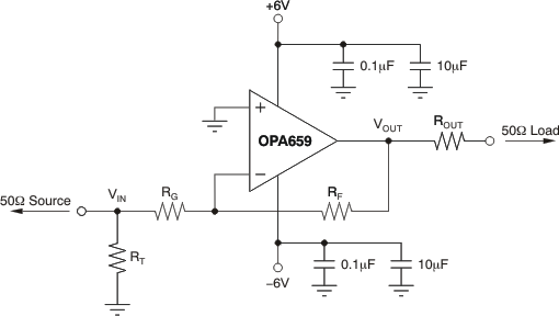 Figure 37. General Inverting Test Circuit
The inverting circuit can also use a wide range of resistor values to set the gain; Table 3 lists several recommended resistor values for inverting gains with a 50-Ω input and output match.
Table 3. Resistor Values For Inverting Gains With 50-Ω Input/Output Match
| INVERTING GAIN | RF | RG | RT | ROUT |
|---|---|---|---|---|
| –1 | 249 | 249 | 61.9 | 49.9 |
| –2 | 249 | 124 | 84.5 | 49.9 |
| –5 | 249 | 49.9 | Open | 49.9 |
| –10 | 499 | 49.9 | Open | 49.9 |
Figure 37 shows the noninverting input tied directly to ground. Often, a bias current-cancelling resistor to ground is included here to nullify the DC errors caused by input bias current effects. For a JFET input op amp such as the OPA659, the input bias currents are so low that dc errors caused by input bias currents are negligible. Thus, TI does not recommend a bias current-cancelling resistor at the noninverting input.
9.1.3 Operating Suggestions
9.1.3.1 Setting Resistor Values To Minimize Noise
The OPA659 provides a very low input noise voltage. To take full advantage of this low input noise, designers must pay careful attention to other possible noise contributors. Figure 38 shows the op amp noise analysis model with all the noise terms included. In this model, all the noise terms are taken to be noise voltage or current density terms in either nV/√Hz or pA/√Hz.
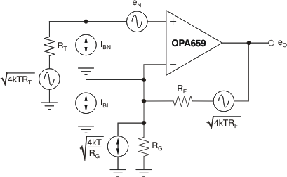 Figure 38. Op Amp Noise Analysis Model
The total output spot noise voltage can be computed as the square root of the squared contributing terms to the output noise voltage. This computation adds all the contributing noise powers at the output by superposition, then takes the square root to arrive at a spot noise voltage. Equation 1 shows the general form for this output noise voltage using the terms shown in Figure 38.

Dividing this expression by the noise gain (GN = 1 + RF/RG) gives the equivalent input-referred spot noise voltage at the noninverting input, as Equation 2 shows.

space
space
Putting high resistor values into Equation 2 can quickly dominate the total equivalent input-referred noise. A source impedance on the noninverting input of 5 kΩ adds a Johnson voltage noise term equal to that of the amplifier alone (8.9 nV/Hz). While the JFET input of the OPA659 is ideal for high source impedance applications in the noninverting configuration of Figure 35 or Figure 36, both the overall bandwidth and noise are limited by high source impedances.
9.1.3.2 Frequency Response Control
Voltage-feedback op amps such as the OPA659 exhibit decreasing signal bandwidth as the signal gain increases. In theory, this relationship is described by the gain bandwidth product (GBP) shown in the Electrical Characteristics. Ideally, dividing the GBP by the noninverting signal gain (also called the Noise Gain, or NG) can predict the closed-loop bandwidth. In practice, this guideline is valid only when the phase margin approaches 90 degrees, as it does in high gain configurations. At low gains (with increased feedback factors), most high-speed amplifiers exhibit a more complex response with lower phase margins. The OPA659 is compensated to give a maximally-flat frequency response at a noninverting gain of +1 (see Figure 35). This compensation results in a typical gain of +1 bandwidth of 650 MHz, far exceeding that predicted by dividing the 350-MHz GBP by 1. Increasing the gain causes the phase margin to approach 90° and the bandwidth to more closely approach the predicted value of (GBP/NG). At a gain of +10, the OPA659 shows the 35-MHz bandwidth predicted using the simple formula and the typical GBP of 350 MHz. Unity-gain stable op amps such as the OPA659 can also be band-limited in gains other than +1 by placing a capacitor across the feedback resistor. For the noninverting configuration of Figure 36, a capacitor across the feedback resistor decreases the gain with frequency down to a gain of +1. For instance, to band-limit a gain of +2 design to 20 MHz, a 32-pF capacitor can be placed in parallel with the 249-Ω feedback resistor. This configuration, however, only decreases the gain from 2 to 1. Using a feedback capacitor to limit the signal bandwidth is more effective in the inverting configuration of Figure 37. Adding that same capacitance to the feedback of Figure 37 sets a pole in the signal frequency response at 20 MHz, but in this case it continues to attenuate the signal gain to less than 1. Note, however, that the noise gain of the circuit is only reduced to a gain of 1 with the addition of the feedback capacitor.
9.1.3.3 Driving Capacitive Loads
One of the most demanding, and yet very common, load conditions for an op amp is capacitive loading. The OPA659 is very robust, but care should be taken with light loading scenarios so that output capacitance does not decrease stability and increase closed-loop frequency response peaking when a capacitive load is placed directly on the output pin. When the amplifier open-loop output resistance is considered, this capacitive load introduces an additional pole in the signal path that can decrease the phase margin. Several external solutions to this problem have been suggested. When the primary considerations are frequency response flatness, pulse response fidelity, and/or distortion, the simplest and most effective solution is to isolate the capacitive load from the feedback loop by inserting a series isolation resistor, RISO, between the amplifier output and the capacitive load. In effect, this resistor isolates the phase shift from the loop gain of the amplifier, thus increasing the phase margin and improving stability. The Typical Characteristics show the recommended RISO versus capacitive load and the resulting frequency response with a 1-kΩ load (see Figure 24). Note that larger RISO values are required for lower capacitive loading. In this case, a design target of a maximally-flat frequency response was used. Lower values of RISO may be used if some peaking can be tolerated. Also, operating at higher gains (instead of the +1 gain used in the Typical Characteristics) requires lower values of RISO for a minimally-peaked frequency response. Parasitic capacitive loads greater than 2pF can begin to degrade the performance of the OPA659. Moreover, long PCB traces, unmatched cables, and connections to multiple devices can easily cause this value to be exceeded. Always consider this effect carefully, and add the recommended series resistor as close as possible to the OPA659 output pin (see the Layout section).
With heavier loads (for example, the 100-Ω load presented in the test circuits and used for testing typical characteristic performance), the OPA659 is very robust; RISO can be as low as 10 Ω with capacitive loads less than 5 pF and continue to show a flat frequency response.
space
space
9.1.3.4 Distortion Performance
The OPA659 is capable of delivering a low distortion signal at high frequencies over a wide range of gains. The distortion plots in the Typical Characteristics show the typical distortion under a wide variety of conditions. Generally, until the fundamental signal reaches very high frequencies or powers, the second harmonic dominates the distortion with a negligible third harmonic component. Focusing then on the second harmonic, increasing the load impedance improves distortion directly. Remember that the total load includes the feedback network: in the noninverting configuration, this network is the sum of RF + RG, while in the inverting configuration the network is only RF (see Figure 36). Increasing the output voltage swing directly increases harmonic distortion. A 6dB increase in output swing generally increases the second harmonic by 12 dB and the third harmonic by 18 dB. Increasing the signal gain also increases the second-harmonic distortion. Again, a 6-dB increase in gain increases the second and third harmonics by about 6 dB, even with a constant output power and frequency. Finally, the distortion increases as the fundamental frequency increases because of the rolloff in the loop gain with frequency. Conversely, the distortion improves going to lower frequencies, down to the dominant open-loop pole at approximately 300 kHz.
Note that power-supply decoupling is critical for harmonic distortion performance. In particular, for optimal second-harmonic performance, the power-supply high-frequency 0.1-μF decoupling capacitors to the positive and negative supply pins should be brought to a single point ground located away from the input pins.
The OPA659 has an extremely low third-order harmonic distortion. This characteristic also shows up in the two-tone, third-order intermodulation spurious (IMD3) response curves (see Figure 19). The third-order spurious levels are extremely low (less than –100 dBc) at low output power levels and frequencies below 10 MHz. The output stage continues to hold these levels low even as the fundamental power reaches higher levels. As with most op amps, the spurious intermodulation powers do not increase as predicted by a traditional intercept model. As the fundamental power level increases, the dynamic range does not decrease significantly. For two tones centered at 10 MHz, with –2 dBm/tone into a matched 50-Ω load (that is, 0.5 VPP for each tone at the load, which requires 2 VPP for the overall two-tone envelope at the output pin), the Typical Characteristics show a 96-dBc difference between the test tones and the third-order intermodulation spurious levels. This exceptional performance improves further when operating at lower frequencies and/or higher load impedances.
9.2 Typical Application
The high GBP and low input voltage and current noise for the OPA659 make it an ideal wideband, transimpedance amplifier for low to moderate transimpedance gains. Higher transimpedance gains (above 100 kΩ) can benefit from the low input noise current of a JFET input op amp such as the OPA659. Designs that require high bandwidth from a large area detector can benefit from the low input voltage noise for the OPA659.
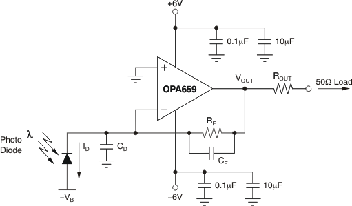 Figure 39. Wideband, Low-Noise, Transimpedance Amplifier (TIA)
9.2.1 Design Requirements
Design a high-gain transimpedance amplifier with the specifications shown in Table 4.
Table 4. Design Parameters
| PARAMETER | VALUE |
|---|---|
| Closed loop bandwidth (MHz) | 7.5 MHz |
| Transimpedance gain | 10 KΩ |
| Photodiode capacitance | 100 pF |
9.2.2 Detailed Design Procedure
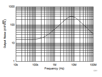
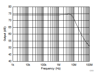
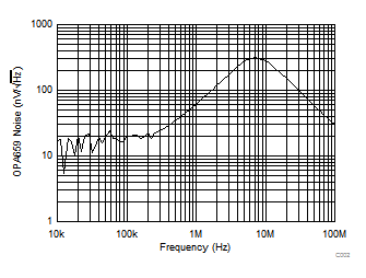
The input voltage noise of a transimpedance amplifier is peaked up over frequency by the diode source capacitance, and in many cases, may become the limiting factor to input sensitivity. The key elements to the design are the expected diode capacitance (CD) with the reverse bias voltage (–VB) applied, the desired transimpedance gain, RF, and the GBP for the OPA659 (350 MHz). Figure 39 shows a general transimpedance amplifier circuit, or TIA, using the OPA659. Given the source diode capacitance plus parasitic input capacitance for the OPA659, the transimpedance gain, and known GBP, the feedback capacitor value, CF, may be calculated to avoid excessive peaking in the frequency response.
To achieve a maximally flat second-order Butterworth frequency response, the feedback pole should be set to:

For example, adding the common mode and differential mode input capacitance (0.7 + 2.8 = 3.5)pF to the diode source with the 20-pF capacitance, and targeting a 100-kΩ transimpedance gain using the 350-MHz GBP for the OPA659, requires a feedback pole set to 3.44 MHz. This pole in turn requires a total feedback capacitance of 0.46 pF. Typical surface mount resistors have a parasitic capacitance of 0.2 pF, leaving the required 0.26 pF value to achieve the required feedback pole. This calculation gives an approximate 4.9 MHz, –3-dB bandwidth computed by:

Table 5 lists the calculated component values and –3-dB bandwidths for various TIA gains and diode capacitance.
Table 5. OPA659 TIA Component Values and Bandwidth for Various Diode Capacitance and Gains
| CD | RF | CF | f–3dB |
|---|---|---|---|
| CDIODE = 10 pF | |||
| 13.5 pF | 1 kΩ | 3.50 pF | 64.24 MHz |
| 13.5 pF | 10 kΩ | 1.11 pF | 20.31 MHz |
| 13.5 pF | 100 kΩ | 0.35 pF | 6.42 MHz |
| 13.5 pF | 1 MΩ | 0.11 pF | 2.03 MHz |
| CDIODE = 20 pF | |||
| 23.5 pF | 1 kΩ | 4.62 pF | 48.69 MHz |
| 23.5 pF | 10 kΩ | 1.46 pF | 15.40 MHz |
| 23.5 pF | 100 kΩ | 0.46 pF | 4.87 MHz |
| 23.5 pF | 1 MΩ | 0.15 pF | 1.54 MHz |
| CDIODE = 50 pF | |||
| 53.5 pF | 1 kΩ | 6.98 pF | 32.27 MHz |
| 53.5 pF | 10 kΩ | 2.21 pF | 10.20 MHz |
| 53.5 pF | 100 kΩ | 0.70 pF | 3.23 MHz |
| 53.5 pF | 1 MΩ | 0.22 pF | 1.02 MHz |
| CDIODE = 100 pF | |||
| 103.5 pF | 1kΩ | 9.70pF | 23.20MHz |
| 103.5 pF | 10kΩ | 3.07pF | 7.34MHz |
| 103.5 pF | 100kΩ | 0.97pF | 2.32MHz |
| 103.5 pF | 1MΩ | 0.31pF | 0.73MHz |
9.2.3 Application Curves
