JAJSDO2C August 2017 – October 2023 OPA838
PRODUCTION DATA
- 1
- 1 特長
- 2 アプリケーション
- 3 概要
- 4 Revision History
- 5 Device Comparison Table
- 6 Pin Configuration and Functions
-
7 Specifications
- 7.1 Absolute Maximum Ratings
- 7.2 ESD Ratings
- 7.3 Recommended Operating Conditions
- 7.4 Thermal Information
- 7.5 Electrical Characteristics: VS = 5 V
- 7.6 Electrical Characteristics: VS = 3 V
- 7.7 Typical Characteristics: VS = 5 V
- 7.8 Typical Characteristics: VS = 3 V
- 7.9 Typical Characteristics: Over Supply Range
- 8 Detailed Description
- 9 Application and Implementation
- 10Device and Documentation Support
- Mechanical, Packaging, and Orderable Information
パッケージ・オプション
メカニカル・データ(パッケージ|ピン)
サーマルパッド・メカニカル・データ
発注情報
8.3.5 Driving Capacitive Loads
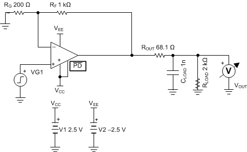
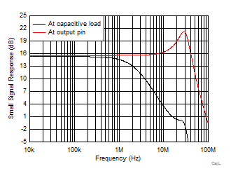
The OPA838 can drive small capacitive loads directly without oscillation (less than 6@pF). When driving capacitive loads greater than 6 pF, Figure 7-49 illustrates the recommended ROUT vs capacitor load parametric on gains. At higher gains, the amplifier starts with greater phase margin into a resistive load and can operate with lower ROUT for a given capacitive load. Without ROUT, output capacitance interacts with the output impedance of the amplifier, which causes phase shift in the loop gain of the amplifier that reduces the phase margin. This causes peaking in the frequency response with overshoot and ringing in the pulse response. Figure 7-49 targets a 30° phase margin for the OPA838. A 30° phase margin produces a 5.7‑dB peaking in the frequency response at the amplifier output pin that is rolled off by the output RC pole; see Figure 8-7. This peaking can cause clipping for large signals driving a capacitive load. Increasing the ROUT value can reduce the peaking at the cost of a more band-limited overall response.
 Figure 8-6 ROUT versus CL Test Circuit
 Figure 8-7 Frequency Response to Output
Pin and Capacitive Load