JAJSF85A April   2018  – July 2018 OPA858

PRODUCTION DATA.  

  1. 特長
  2. アプリケーション
  3. 概要
    1.     Device Images
      1.      高速タイム・オブ・フライト・レシーバ
      2.      フォトダイオード容量と帯域幅およびノイズとの関係
  4. 改訂履歴
  5. Device Comparison Table
  6. Pin Configuration and Functions
    1.     Pin Functions
  7. Specifications
    1. 7.1 Absolute Maximum Ratings
    2. 7.2 ESD Ratings
    3. 7.3 Recommended Operating Conditions
    4. 7.4 Thermal Information
    5. 7.5 Electrical Characteristics
    6. 7.6 Typical Characteristics
  8. Parameter Measurement Information
    1. 8.1 Parameter Measurement Information
  9. Detailed Description
    1. 9.1 Overview
    2. 9.2 Functional Block Diagram
    3. 9.3 Feature Description
      1. 9.3.1 Input and ESD Protection
      2. 9.3.2 Feedback Pin
      3. 9.3.3 Wide Gain-Bandwidth Product
      4. 9.3.4 Slew Rate and Output Stage
      5. 9.3.5 Current Noise
    4. 9.4 Device Functional Modes
      1. 9.4.1 Split-Supply and Single-Supply Operation
      2. 9.4.2 Power-Down Mode
  10. 10Application and Implementation
    1. 10.1 Application Information
      1. 10.1.1 Using the OPA858 as a Transimpedance Amplifier
    2. 10.2 Typical Application
      1. 10.2.1 Design Requirements
      2. 10.2.2 Detailed Design Procedure
      3. 10.2.3 Application Curves
  11. 11Power Supply Recommendations
  12. 12Layout
    1. 12.1 Layout Guidelines
    2. 12.2 Layout Example
  13. 13デバイスおよびドキュメントのサポート
    1. 13.1 ドキュメントの更新通知を受け取る方法
    2. 13.2 コミュニティ・リソース
    3. 13.3 商標
    4. 13.4 静電気放電に関する注意事項
    5. 13.5 Glossary
  14. 14メカニカル、パッケージ、および注文情報

パッケージ・オプション

メカニカル・データ(パッケージ|ピン)
サーマルパッド・メカニカル・データ
発注情報

Current Noise

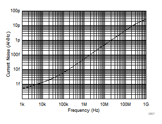
The input impedance of CMOS and JFET input amplifiers at low frequencies exceed several GΩs. However, at higher frequencies, the transistors parasitic capacitance to the drain, source, and substrate reduces the impedance. The high impedance at low frequencies eliminates any bias current and the associated shot noise. At higher frequencies, the input current noise increases (see Figure 53) as a result of capacitive coupling between the CMOS gate oxide and the underlying transistor channel. This phenomenon is a natural artifact of the construction of the transistor and is unavoidable.
OPA858 D607_SBOS852.gifFigure 53. Input Current Noise (IBN and IBI) vs Frequency