JAJSDR9 August 2017 OPT3007
PRODUCTION DATA.
- 1 特長
- 2 アプリケーション
- 3 概要
- 4 改訂履歴
- 5 Pin Configuration and Functions
- 6 Specifications
-
7 Detailed Description
- 7.1 Overview
- 7.2 Functional Block Diagram
- 7.3 Feature Description
- 7.4 Device Functional Modes
- 7.5 Programming
- 7.6
Register Maps
- 7.6.1
Internal Registers
- 7.6.1.1
Register Descriptions
- 7.6.1.1.1 Result Register (Offset = 00h)
- 7.6.1.1.2 Configuration Register (Offset = 01h) [Reset = C810h]
- 7.6.1.1.3 Low-Limit Register (Offset = 02h) [Reset = C0000h]
- 7.6.1.1.4 High-Limit Register (Offset = 03h) [Reset = BFFFh]
- 7.6.1.1.5 Manufacturer ID Register (Offset = 7Eh) [Reset = 5449h]
- 7.6.1.1.6 Device ID Register (Offset = 7Fh) [Reset = 3001h]
- 7.6.1.1
Register Descriptions
- 7.6.1
Internal Registers
- 8 Application and Implementation
- 9 Power-Supply Recommendations
- 10Layout
- 11デバイスおよびドキュメントのサポート
- 12メカニカル、パッケージ、および注文情報
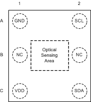
5 Pin Configuration and Functions
YMF Package
6-Pin PicoStar
Top View

Pin Functions
| PIN | TYPE | DESCRIPTION | |
|---|---|---|---|
| NO. | NAME | ||
| A1 | GND | Power | Ground |
| B1 | NC(1) | — | No connection required |
| C1 | VDD | Power | Device power. Connect to a 1.6-V to 3.6-V supply. |
| A2 | SCL | Digital input | I2C clock. Connect with a 10-kΩ resistor to a 1.6-V to 5.5-V supply. |
| B2 | NC(1) | — | No connection required |
| C2 | SDA | Digital input/output | I2C data. Connect with a 10-kΩ resistor to a 1.6-V to 5.5-V supply. |
(1) OPT3007 device has a fixed addressing scheme (see Serial Bus Address). This enables pin B1 and B2 to remain unconnected which enables creating a bigger opening for the sensor active area can be made wider for optimal device performance.