SBAS448B October 2008 – August 2015 PCM1690
PRODUCTION DATA.
- 1 Features
- 2 Applications
- 3 Description
- 4 Revision History
- 5 Pin Configuration and Functions
-
6 Specifications
- 6.1 Absolute Maximum Ratings
- 6.2 ESD Ratings
- 6.3 Recommended Operating Conditions
- 6.4 Thermal Information
- 6.5 Electrical Characteristics: Digital Input/Output
- 6.6 Electrical Characteristics: DAC
- 6.7 Electrical Characteristics: Power-Supply Requirements
- 6.8 System Clock Timing Requirements
- 6.9 Audio Interface Timing Requirements for Left-Justified, Right-Justified, and I2S Data Formats
- 6.10 Audio Interface Timing Requirements for DSP and TDM Data Formats
- 6.11 Three-Wire Serial Control Interface Timing Requirements
- 6.12 SCL and SDA Control Interface Timing Requirements
- 6.13 Typical Characteristics
-
7 Detailed Description
- 7.1 Overview
- 7.2 Functional Block Diagram
- 7.3
Feature Description
- 7.3.1 Analog Outputs
- 7.3.2 Voltage Reference VCOM
- 7.3.3 System Clock Input
- 7.3.4 Sampling Mode
- 7.3.5 Reset Operation
- 7.3.6 Zero Flag
- 7.3.7 AMUTE Control
- 7.3.8 Three-Wire (SPI) Serial Control
- 7.3.9 Control Data Word Format
- 7.3.10 Register Write Operation
- 7.3.11 Two-Wire (I2C) Serial Control
- 7.3.12 Packet Protocol
- 7.3.13 Write Operation
- 7.3.14 Read Operation
- 7.3.15 Timing Requirements: SCL and SDA
- 7.4 Device Functional Modes
- 7.5 Register Maps
- 8 Application and Implementation
- 9 Power Supply Recommendations
- 10Layout
- 11Device and Documentation Support
- 12Mechanical, Packaging, and Orderable Information
パッケージ・オプション
デバイスごとのパッケージ図は、PDF版データシートをご参照ください。
メカニカル・データ(パッケージ|ピン)
- DCA|48
サーマルパッド・メカニカル・データ
- DCA|48
発注情報
6 Specifications
6.1 Absolute Maximum Ratings
Over operating free-air temperature range (unless otherwise noted).(1)| PARAMETER | MIN | MAX | UNIT | |
|---|---|---|---|---|
| Supply voltage | VCC1, VCC2 | –0.3 | 6.5 | V |
| VDD | –0.3 | 4 | V | |
| Ground voltage differences | AGND1, AGND2, DGND | –0.1 | 0.1 | V |
| Supply voltage differences | VCC1, VCC2 | –0.1 | 0.1 | V |
| Digital input voltage | RST, TEST, MS, MC, MD, SCKI, AMUTEI, AMUTEO | –0.3 | 6.5 | V |
| BCK, LRCK, DIN1/2/3/4, MODE, ZERO1, ZERO2 | –0.3 | (VDD + 0.3) < 4 | V | |
| Analog input voltage | VCOM, VOUT1–8± | –0.3 | (VCC + 0.3) < 6.5 | V |
| Input current | (all pins except supplies) | –10 | 10 | mA |
| Ambient temperature under bias | –40 | 125 | °C | |
| Junction temperature | 150 | °C | ||
| Lead temperature | (soldering, 5s) | 260 | °C | |
| Package temperature | (IR reflow, peak) | 260 | °C | |
| Storage temperature | Tstg | –55 | 150 | °C |
6.2 ESD Ratings
| VALUE | UNIT | |||
|---|---|---|---|---|
| V(ESD) | Electrostatic discharge | Human body model (HBM), per ANSI/ESDA/JEDEC JS-001(1) | ±1000 | V |
| Charged-device model (CDM), per JEDEC specification JESD22-C101(2) | ±250 | |||
6.3 Recommended Operating Conditions
Over operating free-air temperature range (unless otherwise noted).| MIN | NOM | MAX | UNIT | ||
|---|---|---|---|---|---|
| Analog supply voltage, VCC | 4.5 | 5 | 5.5 | V | |
| Digital supply voltage, VDD | 3 | 3.3 | 3.6 | V | |
| Digital Interface | LVTTL compatible | ||||
| Digital input clock frequency | Sampling frequency, LRCK | 8 | 192 | kHz | |
| System clock frequency, SCKI | 2.048 | 36.864 | MHz | ||
| Analog output voltage | Differential | 8 | VPP | ||
| Analog output load resistance | To AC-coupled GND | 5 | kΩ | ||
| To DC-coupled GND | 15 | kΩ | |||
| Analog output load capacitance | 50 | pF | |||
| Digital output load capacitance | 20 | pF | |||
| Operating free-air temperature | PCM1690 consumer grade | –40 | 25 | 85 | °C |
6.4 Thermal Information
| THERMAL METRIC(1) | PCM1690 | UNIT | |
|---|---|---|---|
| DCA (HTSSOP) | |||
| 48 PINS | |||
| RθJA | Junction-to-ambient thermal resistance | 29.2 | °C/W |
| RθJC(top) | Junction-to-case (top) thermal resistance | 10.2 | °C/W |
| RθJB | Junction-to-board thermal resistance | 10.3 | °C/W |
| ψJT | Junction-to-top characterization parameter | 0.3 | °C/W |
| ψJB | Junction-to-board characterization parameter | 10.2 | °C/W |
| RθJC(bot) | Junction-to-case (bottom) thermal resistance | 0.4 | °C/W |
6.5 Electrical Characteristics: Digital Input/Output
All specifications at TA = 25°C, VCC1 = VCC2 = 5 V, VDD = 3.3 V, fS = 48 kHz, SCKI = 512 fS, 24-bit data, and Sampling Mode = Auto, unless otherwise noted.| PARAMETER | TEST CONDITIONS | MIN | TYP | MAX | UNIT | ||
|---|---|---|---|---|---|---|---|
| DATA FORMAT | |||||||
| fS | Sampling frequency | 8 | 48 | 192 | kHz | ||
| System clock frequency | 128 fS, 192 fS, 256 fS, 384 fS, 512 fS, 768 fS, 1152 fS |
2.048 | 36.864 | MHz | |||
| INPUT LOGIC | |||||||
| VIH | Input logic level, high (BCK, LRCK, and DIN (2)(1)) | 2 | VDD | VDC | |||
| VIL | Input logic level, low (BCK, LRCK, and DIN ((2)(1)) | 0.8 | VDC | ||||
| VIH | Input logic current, high (SCKI, ADR5/ADR1/RSV, MC/SCL/FMT, MD/SDA/DEMP, and AMUTEI(3)(4)) | 2 | 5.5 | VDC | |||
| VIL | Input logic current, low (SCKI, ADR5/ADR1/RSV, MC/SCL/FMT, MD/SDA/DEMP, and AMUTEI(3)(4)) | 0.8 | VDC | ||||
| IIH | Input logic current, high (SCKI, TEST/ADR1/RSV, MC/SCL/FMT, MD/SDA/DEMP, and AMUTEI(1)(3)) | VIN = VDD | ±10 | μA | |||
| IIL | Input logic current, low (SCKI, TEST/ADR1/RSV, MC/SCL/FMT, MD/SDA/DEMP, and AMUTEI(1)(3)) | VIN = 0 V | ±10 | μA | |||
| IIH | Input logic current, high (BCK, LRCK, REST, MSI/ADR0/RSV (2)(4)) | VIN = VDD | 65 | 100 | μA | ||
| IIL | Input logic current, high (BCK, LRCK, REST, MSI/ADR0/RSV (2)(4)) | VIN = 0 V | ±10 | μA | |||
| OUTPUT LOGIC | |||||||
| VOH | Output logic level, high (ZERO1 and ZERO2(5)) | IOUT = –4 mA | 2.4 | VDC | |||
| VOL | Output logic level, low (ZERO1 and ZERO2(5)(6) ) | IOUT = +4 mA | 0.4 | VDC | |||
| REFERENCE OUTPUT | |||||||
| VCOM output voltage | 0.5 × VCC1 | V | |||||
| VCOM output impedance | 7.5 | kΩ | |||||
| Allowable VCOM output source/sink current | 1 | μA | |||||
6.6 Electrical Characteristics: DAC
All specifications at TA = 25°C, VCC1 = VCC2 = 5 V, VDD = 3.3 V, fS = 48 kHz, SCKI = 512 fS, 24-bit data, and Sampling Mode = Auto, unless otherwise noted.| PARAMETER | TEST CONDITIONS | MIN | TYP | MAX | UNIT | ||
|---|---|---|---|---|---|---|---|
| RESOLUTION | 16 | 24 | Bits | ||||
| DC ACCURACY | |||||||
| Gain mismatch channel-to-channel | ±2 | ±6 | % of FSR | ||||
| Gain error | ±2 | ±6 | % of FSR | ||||
| Bipolar zero error | ±1 | % of FSR | |||||
| DYNAMIC PERFORMANCE(1)(2) | |||||||
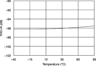
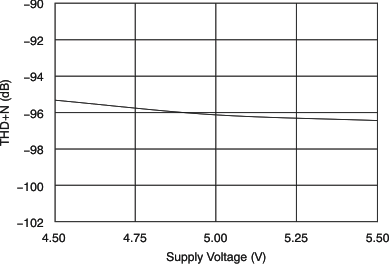
| THD+N | Total harmonic distortion + noise | fS = 48 kHz, VOUT = 0 dB | –94 | –88 | dB | ||
| fS = 96 kHz, VOUT = 0 dB | –94 | dB | |||||
| fS = 192 kHz, VOUT = 0 dB | –94 | dB | |||||
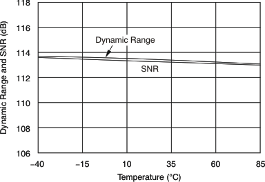
| Dynamic range | fS = 48 kHz, EIAJ, A-weighted | 106 | 113 | dB | |||
| fS = 96 kHz, EIAJ, A-weighted | 113 | dB | |||||
| fS = 192 kHz, EIAJ, A-weighted | 113 | dB | |||||
| SNR | Sighnal-to-noise ratio | fS = 48 kHz, EIAJ, A-weighted | 106 | 113 | dB | ||
| fS = 96 kHz, EIAJ, A-weighted | 113 | dB | |||||
| fS = 192 kHz, EIAJ, A-weighted | 113 | dB | |||||
| Channel separation (between one channel and others) |
fS = 48 kHz | 103 | 109 | dB | |||
| fS = 96 kHz | 109 | dB | |||||
| fS = 192 kHz | 108 | dB | |||||
| ANALOG OUTPUT | |||||||
| Output voltage | Differential | 1.6 × VCC1 | VPP | ||||
| Center voltage | 0.5 × VCC1 | V | |||||
| Load impedance | To AC-coupled GND(3) | 5 | kΩ | ||||
| To DC-coupled GND(3) | 15 | kΩ | |||||
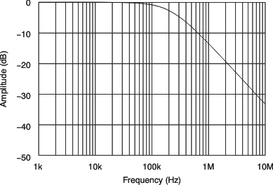
| LPF frequency response | f = 20 kHz | –0.04 | dB | ||||
| f = 44 kHz | –0.18 | dB | |||||
| DIGITAL FILTER PERFORMANCE WITH SHARP ROLL-OFF | |||||||
| Passband (single, dual) | Except SCKI = 128 fS and 192 fS | 0.454 × fS | Hz | ||||
| SCKI = 128 fS and 192 fS | 0.432 × fS | Hz | |||||
| Passband (quad) | 0.432 × fS | Hz | |||||
| Stop band (single, dual) | Except SCKI = 128 fS and 192 fS | 0.546 × fS | Hz | ||||
| SCKI = 128 fS and 192 fS | 0.569 × fS | Hz | |||||
| Stop band (quad) | 0.569 × fS | Hz | |||||
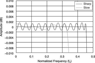
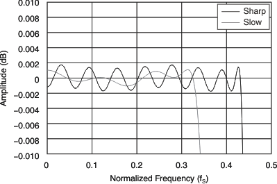
| Passband ripple | < 0.454 × fS, 0.432 × fS | ±0.0018 | dB | ||||
| Stop band attenuation | > 0.546 × fS, 0.569 × fS | –75 | dB | ||||
| DIGITAL FILTER PERFORMANCE WITH SLOW ROLL-OFF | |||||||
| Passband | 0.328 × fS | Hz | |||||
| Stop band | 0.673 × fS | Hz | |||||
| Passband ripple | < 0.328 × fS | ±0.0013 | dB | ||||
| Stop band attenuation | > 0.673 × fS | –75 | dB | ||||
| DIGITAL FILTER PERFORMANCE | |||||||
| Group delay time (single, dual) | Except SCKI = 128 fS and 192 fS | 28/fS | s | ||||
| SCKI = 128 fS and 192 fS | 19/fS | s | |||||
| Group delay time (quad) | 19/fS | s | |||||
| De-emphasis error | ±0.1 | dB | |||||
6.7 Electrical Characteristics: Power-Supply Requirements
All specifications at TA = 25°C, VCC1 = VCC2 = 5 V, VDD = 3.3 V, fS = 48 kHz, SCKI = 512 fS, 24-bit data, and Sampling Mode = Auto, unless otherwise noted.| PARAMETER | TEST CONDITIONS | MIN | TYP | MAX | UNIT | |||
|---|---|---|---|---|---|---|---|---|
| POWER-SUPPLY REQUIREMENTS | ||||||||
| VCC1/2 | Voltage range | 4.5 | 5 | 5.5 | VDC | |||
| VDD | 3 | 3.3 | 3.6 | VDC | ||||
| ICC | Supply current | fS = 48 kHz | 74 | 110 | mA | |||
| fS = 192 kHz | 74 | mA | ||||||
| Full power-down(1) | 170 | μA | ||||||
| fS = 48 kHz | 57 | 90 | mA | |||||
| IDD | fS = 192 kHz | 76 | mA | |||||
| Full power-down(1) | 60 | μA | ||||||
| Power dissipation | fS = 48 kHz fS = 192 kHz Full power-down(1) | 558 | 847 | mW | ||||
| 621 | mW | |||||||
| 1.05 | mW | |||||||
| TEMPERATURE RANGE | ||||||||
| Operating temperature | PCM1690 Consumer grade | –40 | 85 | °C | ||||
6.8 System Clock Timing Requirements
(see Figure 1)| MIN | MAX | UNIT | ||
|---|---|---|---|---|
| tSCY | System clock cycle time | 27 | ns | |
| tSCH | System clock width high | 10 | ns | |
| tSCL | System clock width low | 10 | ns | |
| — | System clock duty cycle | 40% | 60% | |
6.9 Audio Interface Timing Requirements for Left-Justified, Right-Justified, and I2S Data Formats
(see Figure 2)| MIN | MAX | UNIT | ||
|---|---|---|---|---|
| tBCY | BCK cycle time | 75 | ns | |
| tBCH | BCK pulse width high | 35 | ns | |
| tBCL | BCK pulse width low | 35 | ns | |
| tLRS | LRCK set-up time to BCK rising edge | 10 | ns | |
| tLRH | LRCK hold time to BCK rising edge | 10 | ns | |
| tDIS | DIN1/2/3/4 set-up time to BCK rising edge | 10 | ns | |
| tDIH | DIN1/2/3/4 hold time to BCK rising edge | 10 | ns | |
6.10 Audio Interface Timing Requirements for DSP and TDM Data Formats
(see Figure 3)| MIN | MAX | UNIT | ||
|---|---|---|---|---|
| tBCY | BCK cycle time | 40 | ns | |
| tBCH | BCK pulse width high | 15 | ns | |
| tBCL | BCK pulse width low | 15 | ns | |
| tLRW | LRCK pulse width high (DSP format) | tBCY | tBCY | |
| LRCK pulse width high (TDM format) | tBCY | 1/fS – tBCY | ||
| tLRS | LRCK set-up time to BCK rising edge | 10 | ns | |
| tLRH | LRCK hold time to BCK rising edge | 10 | ns | |
| tDIS | DIN1/2/3/4 set-up time to BCK rising edge | 10 | ns | |
| tDIH | DIN1/2/3/4 hold time to BCK rising edge | 10 | ns | |
6.11 Three-Wire Serial Control Interface Timing Requirements
(see Figure 4)| MIN | MAX | UNIT | ||
|---|---|---|---|---|
| tMCY | MC pulse cycle time | 100 | ns | |
| tMCL | MC low-level time | 40 | ns | |
| tMCH | MC high-level time | 40 | ns | |
| tMHH | MS high-level time | tMCY | ns | |
| tMSS | MS falling edge to MC rising edge | 30 | ns | |
| tMSH | MS rising edge from MC rising edge for LSB | 15 | ns | |
| tMDH | MD hold time | 15 | ns | |
| tMDS | MD set-up time | 15 | ns | |
6.12 SCL and SDA Control Interface Timing Requirements
(see Figure 5)| STANDARD MODE | FAST MODE | UNIT | ||||
|---|---|---|---|---|---|---|
| MIN | MAX | MIN | MAX | |||
| fSCL | SCL clock frequency | 100 | 400 | kHz | ||
| tBUF | Bus free time between STOP and START condition | 4.7 | 1.3 | μs | ||
| tLOW | Low period of the SCL clock | 4.7 | 1.3 | μs | ||
| tHI | High period of the SCL clock | 4 | 0.6 | μs | ||
| tS-SU | Set-up time for START/Repeated START condition | 4.7 | 0.6 | μs | ||
| tS-HD | Hold time for START/Repeated START condition | 4.0 | 0.6 | μs | ||
| tD-SU | Data set-up time | 250 | 100 | ns | ||
| tD-HD | Data hold time | 0 | 3450 | 0 | 900 | ns |
| tSCL-R | Rise time of SCL signal | 1000 | 20 + 0.1 CB | 300 | ns | |
| tSCL-F | Fall time of SCL signal | 1000 | 20 + 0.1 CB | 300 | ns | |
| tSDA-R | Rise time of SDA signal | 1000 | 20 + 0.1 CB | 300 | ns | |
| tSDA-F | Fall time of SDA signal | 1000 | 20 + 0.1 CB | 300 | ns | |
| tP-SU | Set-up time for STOP condition | 4 | 0.6 | μs | ||
| tGW | Allowable glitch width | N/A | 50 | |||
| CB | Capacitive load for SDA and SCL line | 400 | 100 | pF | ||
| VNH | Noise margin at high level for each connected device (including hysteresis) |
0.2 × VDD | 0.2 × VDD | V | ||
| VNL | Noise margin at low level for each connected device (including hysteresis) |
0.1 × VDD | 0.1 × VDD | V | ||
| VHYS | Hysteresis of Schmitt trigger input | N/A | 0.05 × VDD | V | ||
 Figure 1. System Clock Timing Requirements
 Figure 2. Audio Interface Timing Requirements for Left-Justified, Right-Justified, and I2S Data Formats
 Figure 3. Audio Interface Timing Requirements for DSP and TDM Data Formats
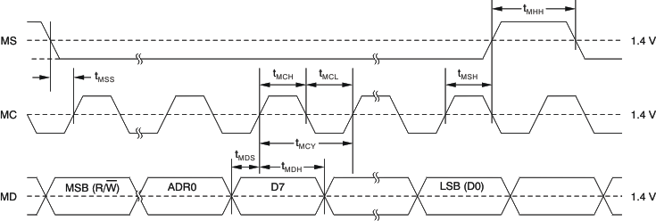 Figure 4. Three-Wire Serial Control Interface Timing
 Figure 5. SCL and SDA Control Interface Timing
6.13 Typical Characteristics
6.13.1 Digital Filter
All specifications at TA = 25°C, VCC1 = VCC2 = 5 V, VDD = 3.3 V, fS = 48 kHz, SCKI = 512 fS, 24-bit data, and Sampling Mode = Auto, unless otherwise noted.

(Single Rate)
(Dual Rate)
(Quad Rate)
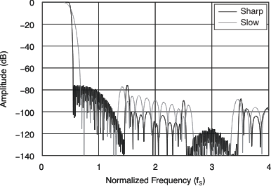
(Dual Rate)
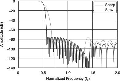
(Quad Rate)
6.13.2 Digital De-Emphasis Filter
All specifications at TA = 25°C, VCC1 = VCC2 = 5 V, VDD = 3.3 V, fS = 48 kHz, SCKI = 512 fS, 24-bit data, and Sampling Mode = Auto, unless otherwise noted.
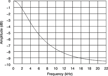
| fS = 48 kHz |
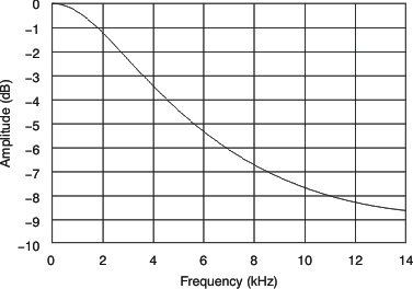
| fS = 32 kHz |
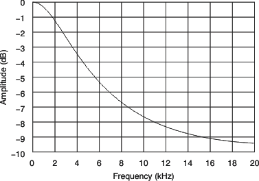
| fS = 44.1 kHz |
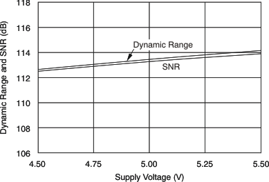
6.13.3 Dynamic Performance
All specifications at TA = 25°C, VCC1 = VCC2 = 5 V, VDD = 3.3 V, fS = 48 kHz, SCKI = 512 fS, 24-bit data, and Sampling Mode = Auto, unless otherwise noted.
6.13.4 Output Spectrum
All specifications at TA = 25°C, VCC1 = VCC2 = 5 V, VDD = 3.3 V, fS = 48 kHz, SCKI = 512 fS, 24-bit data, and Sampling Mode = Auto, unless otherwise noted.
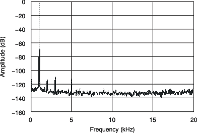
| 0 dB, N = 32768 |
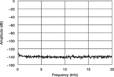
| BPZ, N = 32768 |
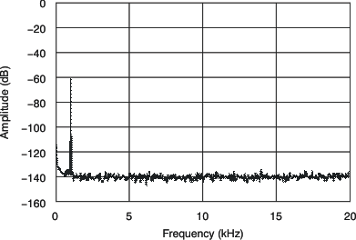
| –60 dB, N = 32768 |