SBFS036B May 2015 – August 2015 PCM2704C , PCM2705C , PCM2706C
PRODUCTION DATA.
- 1 Features
- 2 Applications
- 3 Description
- 4 Revision History
- 5 Device Comparison Table
- 6 Pin Configuration and Functions
-
7 Specifications
- 7.1 Absolute Maximum Ratings
- 7.2 ESD Ratings
- 7.3 Recommended Operating Conditions
- 7.4 Thermal Information: PCM2704C, PCM2705C
- 7.5 Thermal Information: PCM2706C, PCM2707C
- 7.6 Electrical Characteristics: PCM2704CDB, PCM2705CDB, PCM2706CPJT, PCM2707CPJT
- 7.7 Audio Interface Timing Characteristics
- 7.8 Audio Clock Timing Characteristics
- 7.9 External ROM Read Interface Timing Characteristics
- 7.10 SPI Timing Characteristics
- 7.11 Typical Characteristics
- 8 Parameter Measurement Information
-
9 Detailed Description
- 9.1 Overview
- 9.2 Functional Block Diagrams
- 9.3
Feature Description
- 9.3.1 Clock and Reset
- 9.3.2 Operation Mode Selection
- 9.3.3 DAC
- 9.3.4 Digital Audio Interface: S/PDIF Output
- 9.3.5 Digital Audio Interface: I2S Interface Output (PCM2706C/7C)
- 9.3.6 Descriptor Data Modification
- 9.3.7 External ROM Descriptor (PCM2704C/6C)
- 9.3.8 External ROM Example
- 9.3.9 Serial Programming Interface (PCM2705C/7C)
- 9.3.10 USB Host Interface Sequence
- 9.3.11 Operating Environment
- 9.4 Device Functional Modes
- 9.5 Programming
- 9.6 Register Maps
- 10Application and Implementation
- 11Power Supply Recommendations
- 12Layout
- 13Device and Documentation Support
- 14Mechanical, Packaging, and Orderable Information
10 Application and Implementation
NOTE
Information in the following applications sections is not part of the TI component specification, and TI does not warrant its accuracy or completeness. TI’s customers are responsible for determining suitability of components for their purposes. Customers should validate and test their design implementation to confirm system functionality.
10.1 Application Information
The PSEL allows the device to configure for bus-powered mode (High) or self-powered mode (Low). The HOST pin configures the maximum current consumption of the device during bus-powered mode (low: 100 mA, high: 500 mA), or can be used as host detector during self-powered mode. The SSPND flag notifies when the USB input is idle for at least 5 ms; this flag can be used to control or notify subsequent circuits. The device descriptor can be modified by using an external ROM (PCM2704C/6C) or through the SPI port (PCM2705C/7C); this descriptor programming function is only available when PSEL and HOST are high. More functional details can be found in USB Interface.
10.2 Typical Application
10.2.1 Typical Circuit Connection 1: USB Speaker
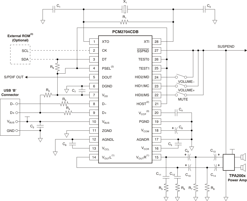
Figure 35 shows a typical circuit connection for an internal-descriptor, bus-powered, 500-mA application.

NOINDENT:
NOTE: X1: 12-MHz crystal resonator. C1, C2: 10- to 33-pF capacitors (depending on load capacitance of crystal resonator). C3to C7: 1-μF ceramic capacitors. C8: 10-μF electrolytic capacitor. C9, C10: 100-μF electrolytic capacitors (depending on tradeoff between required frequency response and discharge time for resume). C11, C12: 0.022-μF ceramic capacitors. C13, C14: 1-μF electrolytic capacitors. R1: 1-MΩ resistor. R2, R9: 1.5-kΩ resistors. R3, R4: 22-Ω resistors. R5, R6: 16-Ω resistors. R7, R8: 330-Ω resistors (depending on tradeoff between required THD performance and pop-noise level for suspend).NOINDENT:
Output impedance of VOUTL and VOUTR during suspended mode or lack of power supply is 26 kΩ ±20%, which is the discharge path for C9 and C10.NOINDENT:
Descriptor programming through external ROM is only available when PSEL and HOST are high.NOINDENT:
External ROM power can be supplied from VCCP, but any other active component must not use VCCP, VCCL, VCCR, or VDD as a power source.NOTE
The circuit shown in Figure 35 is for information only. The entire board design should be considered to meet the USB specification as a USB-compliant product.
10.2.1.1 Design Requirements
For this design example, use the parameters listed in Table 10.
Table 10. Design Parameters
| DESIGN PARAMETER | EXAMPLE VALUE |
|---|---|
| Input voltage range | 4.35 V to 5.25 V (USB power) |
| Current | 500 mA (Bus-Powered Max power) |
| Input clock frequency | 11.994 MHz to 12.006 MHz |
10.2.1.2 Detailed Design Procedure
The PCM2704C/5C/6C/7C is a simple design device that can connect directly to a USB port. Only a 3.3-V external regulator is needed (in self-powered mode), and an external ROM for the descriptor programming function (PCM2704C/6C). The switches connected to the HID ports must be normally open. TI recommends placing an output filter such as the one shown in Figure 35. The PCM2704C/5C/6C/7C requires decoupling capacitors on the voltage source pins.
10.2.1.3 Application Curves
For the application curves, see the graphs listed in Table 11.
10.2.2 Typical Circuit Connection 2: Remote Headphone
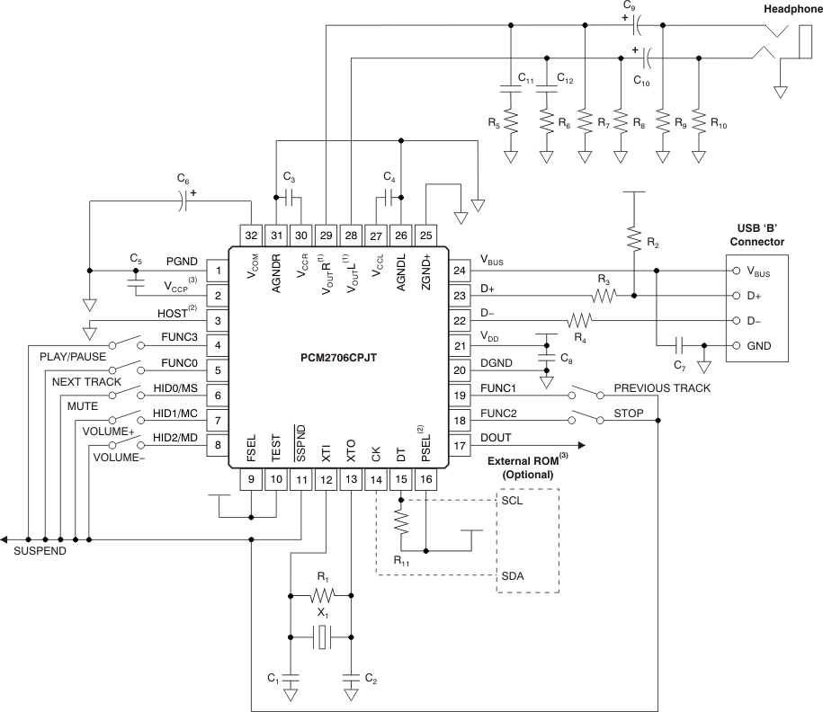
Figure 36 shows a typical circuit connection for a bus-powered, 100-mA headphone with seven HIDs.

NOINDENT:
NOTE: X1: 12-MHz crystal resonator. C1, C2: 10- to 33-pF capacitors (depending on load capacitance of crystal resonator). C3 to C5, C7, C8: 1-μF ceramic capacitors. C6: 10-μF electrolytic capacitor. C9, C10: 100-μF electrolytic capacitors (depending on required frequency response). C11, C12: 0.022-μF ceramic capacitors. R1: 1-MΩ resistor. R2, R11: 1.5-kΩ resistors. R3, R4: 22-Ω resistors. R5, R6: 16-Ω resistors. R7 to R10: 3.3-kΩ resistors.NOINDENT:
Output impedance of VOUTL and VOUTR during suspend mode or lack of power supply is 26 kΩ ±20%, which is the discharge path for C9 and C10.NOINDENT:
Descriptor programming through external ROM is only available when PSEL and HOST are high.NOINDENT:
External ROM power can be supplied from VCCP, but any other active component must not use VCCP, VCCL, VCCR, or VDD as a power source.NOTE
The circuit shown in Figure 36 is for information only. The entire board design should be considered to meet the USB specification as a USB-compliant product.
10.2.2.1 Design Requirements
For this design example, use the parameters listed in Table 12.
Table 12. Design Parameters
| DESIGN PARAMETER | EXAMPLE VALUE |
|---|---|
| Input voltage range | 4.35 V to 5.25 V (USB power) |
| Current | 100 mA (Bus-Powered Max power) |
| Input clock frequency | 11.994 MHz to 12.006 MHz |
10.2.2.2 Detailed Design Procedure
A general detailed design procedure is explained in Detailed Design Procedure.
10.2.2.3 Application Curves
For the application curves, see the graphs listed in Table 11.
10.2.3 Typical Circuit Connection 3: DSP Surround Processing Amplifier
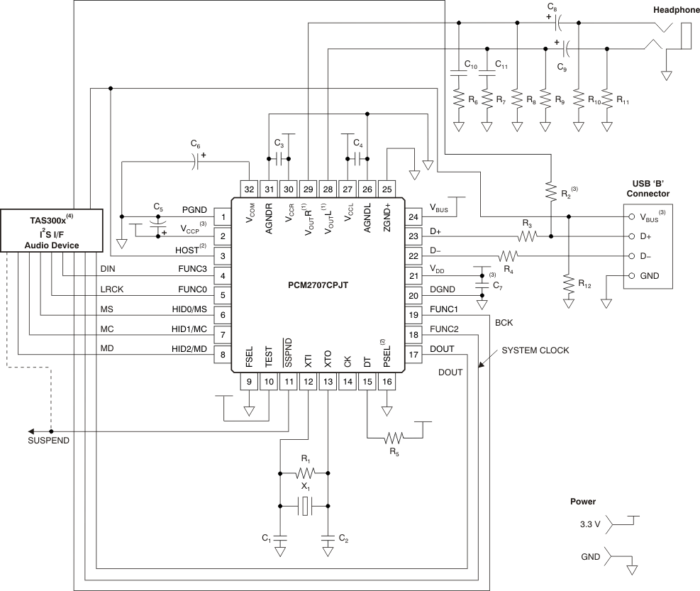
Figure 37 shows a typical circuit connection for an I2S- and SPI-enabled self-powered application.

NOINDENT:
NOTE: X1: 12-MHz crystal resonator. C1, C2: 10- to 33-pF capacitors (depending on load capacitance of crystal resonator). C3, C4: 1-μF ceramic capacitors. C5, C7: 0.1-μF ceramic capacitor and 10-μF electrolytic capacitor. C6: 10-μF electrolytic capacitors. C8, C9: 100-μF electrolytic capacitors (depending on required frequency response). C10, C11: 0.022-μF ceramic capacitors. R1, R12: 1-MΩ resistors. R2, R5: 1.5-kΩ resistors. R3, R4: 22-Ω resistors. R6, R7: 16-Ω resistors. R8to R11: 3.3-kΩ resistors.NOINDENT:
Output impedance of VOUTL and VOUTR during suspend mode or lack of power supply is 26 kΩ ±20%, which is the discharge path for C8 and C9.NOINDENT:
Descriptor programming through SPI is only available when PSEL and HOST are high.NOINDENT:
D+ pullup must not be activated (high: 3.3 V) while the device is detached from USB or power supply is not applied on VDD and VCCx. VBUS of USB (5 V) can be used to detect USB power status.NOINDENT:
MS must be high until the PCM2707C power supply is ready and the SPI host (the DSP) is ready to send data. Also, the SPI host must handle the D+ pullup if the descriptor is programmed through the SPI. D+ pullup must not be activated (high = 3.3 V) before programming of the PCM2707C through the SPI is complete.NOTE
The circuit shown in Figure 37 is for information only. The entire board design should be considered to meet the USB specification as a USB-compliant product.
10.2.3.1 Design Requirements
For this design example, use the parameters listed in Table 13.
Table 13. Design Parameters
| DESIGN PARAMETER | EXAMPLE VALUE |
|---|---|
| Input voltage range | 3 V to 3.6 V |
| Current | 100 mA |
| Input clock frequency | 11.994 MHz to 12.006 MHz |
10.2.3.2 Detailed Design Procedure
A general detailed design procedure is explained in Detailed Design Procedure.
10.2.3.3 Application Curves
For the application curves, see the graphs listed in Table 11.