SBOS218D December   2001  – May 2016 PGA2311

PRODUCTION DATA.  

  1. Features
  2. Applications
  3. Description
  4. Revision History
  5. Pin Configuration and Functions
  6. Specifications
    1. 6.1 Absolute Maximum Ratings
    2. 6.2 ESD Ratings
    3. 6.3 Recommended Operating Conditions
    4. 6.4 Thermal Information
    5. 6.5 Electrical Characteristics
    6. 6.6 Typical Characteristics
  7. Detailed Description
    1. 7.1 Overview
    2. 7.2 Functional Block Diagram
    3. 7.3 Feature Description
      1. 7.3.1 Analog Inputs and Outputs
      2. 7.3.2 Gain Settings
      3. 7.3.3 Daisy-Chaining Multiple PGA2311 Devices
      4. 7.3.4 Zero-Crossing Detection
      5. 7.3.5 MUTE Function
    4. 7.4 Device Functional Modes
      1. 7.4.1 Power-Up State
    5. 7.5 Programming
  8. Application and Implementation
    1. 8.1 Application Information
    2. 8.2 Typical Application
      1. 8.2.1 Design Requirements
      2. 8.2.2 Detailed Design Procedure
      3. 8.2.3 Application Curve
  9. Power Supply Recommendations
  10. 10Layout
    1. 10.1 Layout Guidelines
    2. 10.2 Layout Example
  11. 11Device and Documentation Support
    1. 11.1 Documentation Support
      1. 11.1.1 Related Documentation
    2. 11.2 Community Resources
    3. 11.3 Trademarks
    4. 11.4 Electrostatic Discharge Caution
    5. 11.5 Glossary
  12. 12Mechanical, Packaging, and Orderable Information

パッケージ・オプション

メカニカル・データ(パッケージ|ピン)
サーマルパッド・メカニカル・データ
発注情報

6 Specifications

6.1 Absolute Maximum Ratings

over operating free-air temperature range (unless otherwise noted)(1)
MIN MAX UNIT
Supply voltage VA+ 5.5 V
VA –5.5
VD+ 5.5
VA+ to VD+ < ±0.3
Analog input voltage 0 VA+, VA V
Digital input voltage –0.3 VD+ V
Operating temperature –40 85 °C
Junction temperature 150 °C
Storage temperature, Tstg –65 150 °C
(1) Stresses beyond those listed under Absolute Maximum Ratings may cause permanent damage to the device. These are stress ratings only, which do not imply functional operation of the device at these or any other conditions beyond those indicated under Recommended Operating Conditions. Exposure to absolute-maximum-rated conditions for extended periods may affect device reliability.

6.2 ESD Ratings

VALUE UNIT
PGA2311 in 16-Pin SOIC Package
V(ESD) Electrostatic discharge Human-body model (HBM), per ANSI/ESDA/JEDEC JS-001(1) ±2000 V
Charged-device model (CDM), per JEDEC specification JESD22-C101(2) ±1500
PGA2311 in 16-Pin PDIP Package
V(ESD) Electrostatic discharge Human-body model (HBM), per ANSI/ESDA/JEDEC JS-001(1) ±2000 V
(1) JEDEC document JEP155 states that 500-V HBM allows safe manufacturing with a standard ESD control process.
(2) JEDEC document JEP157 states that 250-V CDM allows safe manufacturing with a standard ESD control process.

6.3 Recommended Operating Conditions

over operating free-air temperature range (unless otherwise noted)
MIN NOM MAX UNIT
VA+ Positive analog power supply 4.75 5 5.25 V
VA Negative analog power supply –4.75 –5 –5.25 V
VD+ Digital power supply 4.75 5 5.25 V
Operating temperature –40 25 85 °C

6.4 Thermal Information

THERMAL METRIC(1) PGA2311 UNIT
N (PDIP) DW (SOIC)
16 PINS 16 PINS
RθJA Junction-to-ambient thermal resistance 39.9 83 °C/W
RθJC(top) Junction-to-case (top) thermal resistance 26.2 44 °C/W
RθJB Junction-to-board thermal resistance 20.1 40.5 °C/W
ψJT Junction-to-top characterization parameter 10.7 11.5 °C/W
ψJB Junction-to-board characterization parameter 19.9 40.2 °C/W
RθJC(bot) Junction-to-case (bottom) thermal resistance °C/W
(1) For more information about traditional and new thermal metrics, see the Semiconductor and IC Package Thermal Metrics application report, SPRA953.

6.5 Electrical Characteristics

At TA = +25°C, VA+ = +5 V, VA− = –5 V, VD+ = +5 V, RL = 100 kΩ, CL = 20 pF, BW measure = 10 Hz to 20 kHz, unless otherwise noted.
PARAMETER TEST CONDITIONS MIN TYP MAX UNIT
DC CHARACTERISTICS
Step size 0.5 dB
Gain error Gain setting = 31.5 dB ±0.05 dB
Gain matching ±0.05 dB
Input resistance 10
Input capacitance PGA2311P, U (U−grade) 3 pF
PGA2311PA, UA (A−grade) 7
AC CHARACTERISTICS
THD+N VIN = 2 Vrms,
f = 1 kHz
PGA2311P,
U (U−grade)
0.0004% 0.001%
PGA2311PA, UA (A−grade) 0.0002% 0.0004%
Dynamic range VIN = AGND, gain = 0 dB 116 120 dB
Voltage range, output PGA2311P, U (U−grade) (VA−) + 1.25 (VA+) –1.25 V
PGA2311PA, UA (A−grade) (VA−) + 1.25 (VA−) − 1.25
Voltage range, input
(without clipping)
2.5 Vrms
Output noise VIN = AGND, gain = 0 dB 2.5 4 μVRMS
Interchannel crosstalk f = 1 kHz –130 dBFS
OUTPUT BUFFER
Offset voltage VIN = AGND, gain = 0 dB 0.25 0.5 mV
Load capacitance stability 100 pF
Short-circuit current 50 mA
Unity-gain bandwidth, small signal 10 MHz
DIGITAL CHARACTERISTICS
VIH High-level input voltage 2 VD+ V
VIL Low-level input voltage –0.3 0.8 V
VOH High-level output voltage IO = 200 μA PGA2311P,
U (U−grade)
(VA+) − 1 V
PGA2311PA, UA (A−grade) (VD+) − 1
VOL Low-level output voltage IO = –3.2 mA 0.4 V
Input leakage current 1 10 µA
SWITCHING CHARACTERISTICS
fSCLK Serial clock (SCLK) frequency 0 6.25 MHz
tPL SCLK pulse duration low 80 ns
tPH SCLK pulse duration high 80 ns
tMI MUTE pulse duration low 2 ms
INPUT TIMING
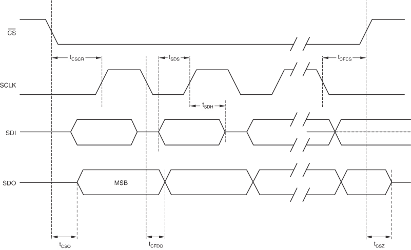
tSDS SDI setup time 20 ns
tSDH SDI hold time 20 ns
tCSCR CS falling to SCLK rising 90 ns
tCFCS SCLK falling to CS rising 35 ns
OUTPUT TIMING
tCSO CS low to SDO active 35 ns
tCFDO SCLK falling to SDO data valid 60 ns
tCSZ CS high to SDO high impedance 100 ns
POWER SUPPLY
Operating voltage VA+ 4.75 5 5.25 V
VA –4.75 –5 –5.25
VD+ 4.75 5 5.25
Quiescent current IA+ VA+ = +5 V 8 10 mA
IA VA– = –5 V 10 12
ID+ VD+ = +5 V 0.5 1
PSRR Power-supply rejection ratio
(250 Hz)
100 dB
TEMPERATURE RANGE
Operating range –40 85 °C
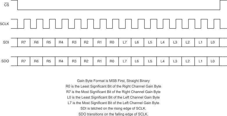
PGA2311 serial_intfc_prot.gif Figure 1. Serial Interface Protocol
PGA2311 serial_intfc_timing_req.gif Figure 2. Serial Interface Timing Requirements
6.6 Typical Characteristics

At TA = +25°C, VA+ = +5 V, VA− = −5 V, VD+ = +5 V, RL = 100 kΩ, CL = 20 pF, BW measure = 10 Hz to 20 kHz, unless otherwise noted. All plots taken with PGA2311 A-grade.
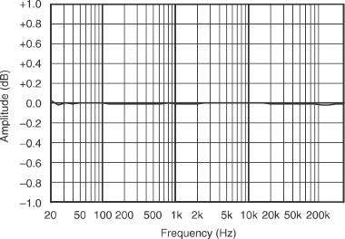
PGA2311 sbos218_typchar1a.gif
Gain = 0 dB, Load = 100 kΩ, VIN = 2 Vrms
Figure 3. Amplitude vs Frequency
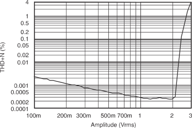
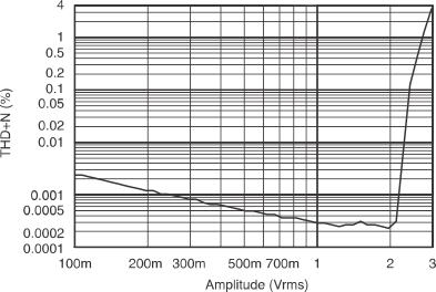
PGA2311 sbos218_typchar3.gif
Gain = 0 dB, Freq = 1 kHz, Load = 600 Ω
Figure 5. THD + N vs Amplitude
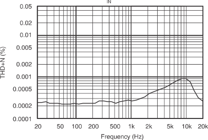
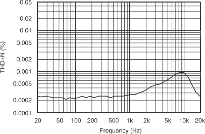
PGA2311 sbos218_typchar5.gif
Gain = 0 dB, VIN = 2 Vrms, Load = 600 Ω
Figure 7. THD + N vs Frequency
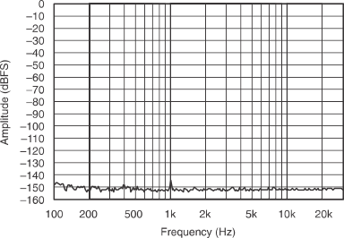
PGA2311 sbos218_typchar1.gif
Figure 9. Crosstalk With FIN = 1 kHz
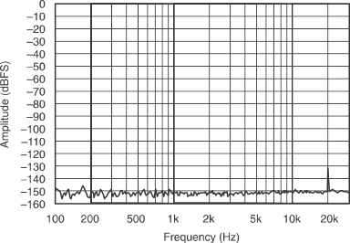
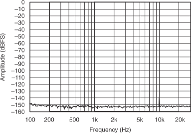
PGA2311 sbos218_typchar9.gif
Figure 11. Crosstalk With FIN = 20 kHz
PGA2311 sbos218_typchar2a.gif
Gain = 0 dB, Freq = 1 kHz, Load = 100 kΩ
Figure 4. THD + N vs Amplitude
PGA2311 sbos218_typchar4.gif
Gain = 0 dB, VIN = 2 Vrms, Load = 100 kΩ
Figure 6. THD + N vs Frequency
PGA2311 sbos218_typchar6.gif
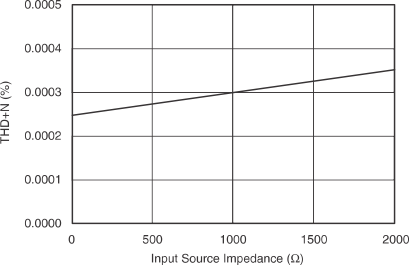
Gain = 0 dB, VIN = 2 Vrms, FIN = 1 kHz
Figure 8. THD + N vs Input Source Impedance
PGA2311 sbos218_typchar2.gif
Figure 10. Crosstalk With FIN = 10 kHz