SBOS218D December 2001 – May 2016 PGA2311
PRODUCTION DATA.
- 1 Features
- 2 Applications
- 3 Description
- 4 Revision History
- 5 Pin Configuration and Functions
- 6 Specifications
- 7 Detailed Description
- 8 Application and Implementation
- 9 Power Supply Recommendations
- 10Layout
- 11Device and Documentation Support
- 12Mechanical, Packaging, and Orderable Information
パッケージ・オプション
メカニカル・データ(パッケージ|ピン)
サーマルパッド・メカニカル・データ
- DW|16
発注情報
7 Detailed Description
7.1 Overview
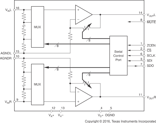
The PGA2311 is a stereo audio volume control that can be used in a wide array of professional and consumer audio equipment. The PGA2311 is fabricated in a sub-micron CMOS process.
The heart of the PGA2311 is a resistor network, an analog switch array, and a high-performance operational amplifier stage. The switches select taps in the resistor network that determine the gain of the amplifier stage. Switch selections are programmed using a serial control port. The serial port allows connection to a wide variety of host controllers. The Functional Block Diagram section shows a model diagram of the PGA2311.
7.2 Functional Block Diagram

7.3 Feature Description
7.3.1 Analog Inputs and Outputs
The PGA2311 includes two independent channels (referred to as the left and right channels). Each channel has a corresponding input and output pin. The input and output pins are unbalanced, or referenced to analog ground (either AGNDR or AGNDL). The inputs are VINR (pin 9) and VINL (pin 16), and the outputs are VOUTR (pin 11) and VOUTL (pin 14). The input and output pins can swing within 1.25 V of the analog power supplies, VA+ (pin 12) and VA− (pin 13). Given VA+ = +5 V and VA− = −5 V, the maximum input or output voltage range is 7.5 Vp-p.
For optimal performance, drive the PGA2311 with a low source impedance. A source impedance of 600 Ω or less is recommended. Source impedances up to 2 kΩ cause minimal degradation of THD+N; see Figure 8 for more details.
7.3.2 Gain Settings
The gain for each channel is set by its corresponding 8-bit code, either R[7:0] or L[7:0] (see Figure 1). The gain code data is straight binary format. If N equals the decimal equivalent of R[7:0] or L[7:0], then the following relationships exist for the gain settings:
- For N = 0: Mute Condition. The input multiplexer is connected to analog ground (AGNDR or AGNDL).
- For N = 1 to 255: Gain (dB) = 31.5 − [0.5 w (255 − N)]
This results in a gain range of +31.5 dB (with N = 255) to −95.5 dB (with N = 1).
Changes in gain setting can be made with or without zero-crossing detection. The operation of the zero-crossing detector and timeout circuitry is discussed in the Zero-Crossing Detection section.
7.3.3 Daisy-Chaining Multiple PGA2311 Devices
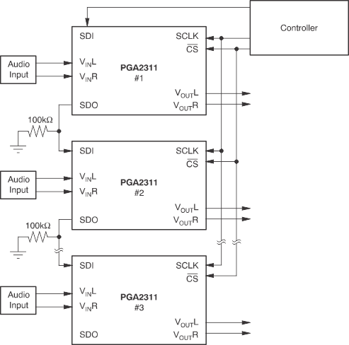
To reduce the number of control signals required to support multiple PGA2311 devices on a printed circuit board (PCB), the serial control port supports daisy-chaining of multiple PGA2311 devices. Figure 12 shows the connection requirements for daisy-chain operation. This arrangement allows a 3-wire serial interface to control many PGA2311 devices.
As shown in Figure 12, the SDO pin from PGA2311 #1 is connected to the SDI input of PGA2311 #2, and is repeated for additional devices. This configuration in turn forms a large shift register, in which gain data can be written for all PGA2311s connected to the serial bus. The length of the shift register is 16 × N bits, where N is equal to the number of PGA2311 devices included in the chain. The CS input must remain LOW for 16 × N SCLK periods, where N is the number of devices connected in the chain, to allow enough SCLK cycles to load all devices.
 Figure 12. Daisy-Chaining Multiple PGA2311 Devices
7.3.4 Zero-Crossing Detection
The PGA2311 includes a zero-crossing detection function for noise-free level transitions. The concept is to change gain settings on a zero-crossing of the input signal, thus minimizing audible glitches. This function is enabled or disabled using the ZCEN input (pin 1). When ZCEN is LOW, zero-crossing detection is disabled. When ZCEN is HIGH, zero-crossing detection is enabled.
The zero-crossing detection takes effect with a change in gain setting for a corresponding channel. The new gain setting is not implemented until either a positive slope zero crossing is detected, or a time-out period of 16 ms has elapsed. In the case of a time-out, the new gain setting takes effect with no attempt to minimize audible artifacts.
7.3.5 MUTE Function
Muting can be achieved by either hardware or software control. Hardware muting is accomplished through the MUTE input, and software muting by loading all zeroes into the volume control register.
MUTE disconnects the internal buffer amplifiers from the output pins and terminates AOUTL and AOUTR with
10-kΩ resistors to ground. The mute is activated with a zero-crossing detection (independent of the zero-cross enable status), or an 16-ms time-out to eliminate any audible clicks or pops. MUTE also initiates an internal offset calibration.
A software mute is implemented by loading all zeroes into the volume control register. The internal amplifier is set to unity gain, with the amplifier input connected to AGND.
7.4 Device Functional Modes
7.4.1 Power-Up State
On power-up, power-up reset is activated for approximately 100 ms, during which the circuit is in hardware MUTE state and all internal flip-flops are reset. At the end of this period, the offset calibration is initiated without any external signals. When this step is complete, the gain byte value for both the left and right channels are set to 00HEX, or the software MUTE condition. The gain remains at this setting until the host controller programs new settings for each channel via the serial control port.
If the power-supply voltage drops below ±3.2 V during normal operation, the circuit enters a hardware MUTE state. A power-up sequence initiates if the power-supply voltage returns to greater than ±3.2 V.
7.5 Programming
The serial control port is used to program the gain settings for the PGA2311. The serial control port includes three input pins and one output pin. The inputs include CS (pin 2), SDI (pin 3), and SCLK (pin 6). The sole output pin is SDO (pin 7).
The CS pin functions as the chip-select input. Data can be written to the PGA2311 only when CS is LOW. SDI is the serial data input pin. Control data are provided as a 16-bit word at the SDI pin, 8 bits each for the left and right channel gain settings.
Data are formatted as MSB first, in straight binary code. SCLK is the serial clock input. Data are clocked into SDI on the rising edge of SCLK.
SDO is the serial data output pin, and used when daisy-chaining multiple PGA2311 devices. Daisy-chain operation is described in the Daisy-Chaining Multiple PGA2311 Devices section. SDO is a tri-state output, and assumes a high-impedance state when CS is HIGH.
The protocol for the serial control port is illustrated in Figure 1; see Figure 2 for detailed timing specifications for the serial control port.