SLOS073G
March 1976 – November 2014
RC4558
PRODUCTION DATA.
1
Features
2
Applications
3
Description
4
Revision History
5
Pin Configuration and Functions
6
Specifications
6.1
Absolute Maximum Ratings
6.2
Handling Ratings
6.3
Recommended Operating Conditions
6.4
Thermal Information
6.5
Electrical Characteristics
6.6
Operating Characteristics
6.7
Typical Characteristics
7
Detailed Description
7.1
Overview
7.2
Functional Block Diagram
7.3
Feature Description
7.3.1
Unity-Gain Bandwidth
7.3.2
Common-Mode Rejection Ratio
7.3.3
Slew Rate
7.4
Device Functional Modes
8
Application and Implementation
8.1
Typical Application
8.1.1
Design Requirements
8.1.2
Detailed Design Procedure
8.1.2.1
Amplifier Selection
8.1.2.2
Passive Component Selection
8.1.3
Application Curves
9
Power Supply Recommendations
10
Layout
10.1
Layout Guidelines
10.2
Layout Example
11
Device and Documentation Support
11.1
Glossary
12
Mechanical, Packaging, and Orderable Information
デバイスごとのパッケージ図は、PDF版データシートをご参照ください。
メカニカル・データ(パッケージ|ピン)
D|8
P|8
PS|8
DGK|8
PW|8
サーマルパッド・メカニカル・データ
PS|8
QFND376
DGK|8
QFND519
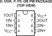
5 Pin Configuration and Functions
Pin Functions
PIN
TYPE
DESCRIPTION
NAME
NO.
1IN+
3
I
Noninverting input
1IN-
2
I
Inverting Input
1OUT
1
O
Output
2IN+
5
I
Noninverting input
2IN-
6
I
Inverting Input
2OUT
7
O
Output
V
CC
+
8
—
Positive Supply
V
CC
-
4
—
Negative Supply