6 Specifications
6.1 Absolute Maximum Ratings
over operating free-air temperature range (unless otherwise noted)(1)
|
MIN |
MAX |
UNIT |
| Supply voltage, VCC(2) |
|
7 |
V |
| Input voltage |
SNx400 and SNxS400 |
|
5.5 |
V |
| SNx4LS00 |
|
7 |
| Junction temperature, TJ |
|
150 |
°C |
| Storage temperature, Tstg |
–65 |
150 |
°C |
(1) Stresses beyond those listed under Absolute Maximum Ratings may cause permanent damage to the device. These are stress ratings only, which do not imply functional operation of the device at these or any other conditions beyond those indicated under Recommended Operating Conditions. Exposure to absolute-maximum-rated conditions for extended periods may affect device reliability.
(2) Voltage values are with respect to network ground terminal.
6.2 ESD Ratings: SN74LS00
|
VALUE |
UNIT |
| V(ESD) |
Electrostatic discharge |
Human-body model (HBM), per ANSI/ESDA/JEDEC JS-001(1) |
±500 |
V |
| Charged-device model (CDM), per JEDEC specification JESD22-C101(2) |
±2000 |
(1) JEDEC document JEP155 states that 500-V HBM allows safe manufacturing with a standard ESD control process. Manufacturing with less than 500-V HBM is possible with the necessary precautions.
(2) JEDEC document JEP157 states that 250-V CDM allows safe manufacturing with a standard ESD control process. Manufacturing with less than 250-V CDM is possible with the necessary precautions. Pins listed as ±2000 V may actually have higher performance. ESD Tested on SN74LS00N package.
6.3 Recommended Operating Conditions
over operating free-air temperature range (unless otherwise noted)
|
MIN |
NOM |
MAX |
UNIT |
| VCC |
Supply voltage |
SN54xx00 |
4.5 |
5 |
5.5 |
V |
| SN74xx00 |
4.75 |
5 |
5.25 |
| VIH |
High-level input voltage |
2 |
|
|
V |
| VIL |
Low-level input voltage |
SNx400, SN7LS400, and SNx4S00 |
|
|
0.8 |
V |
| SN54LS00 |
|
|
0.7 |
| IOH |
High-level output current |
SN5400, SN54LS00, and SN74LS00 |
|
|
–0.4 |
mA |
| SNx4S00 |
|
|
–1 |
| IOL |
Low-level output current |
SNx400 |
|
|
16 |
mA |
| SN5LS400 |
|
|
4 |
| SN7LS400 |
|
|
8 |
| SNx4S00 |
|
|
20 |
| TA |
Operating free-air temperature |
SN54xx00 |
–55 |
|
125 |
°C |
| SN74xx00 |
0 |
|
70 |
6.4 Thermal Information
| THERMAL METRIC(1)(2) |
SN74LS00 |
UNIT |
| D (SOIC) |
DB (SSOP) |
N (PDIP) |
NS (SO) |
| 14 PINS |
14 PINS |
14 PINS |
14 PINS |
| RθJA |
Junction-to-ambient thermal resistance |
90.9 |
102.8 |
54.8 |
89.7 |
°C/W |
| RθJC(top) |
Junction-to-case (top) thermal resistance |
51.9 |
53.3 |
42.1 |
48.1 |
°C/W |
| RθJB |
Junction-to-board thermal resistance |
48 |
53.4 |
34.8 |
50.1 |
°C/W |
| ψJT |
Junction-to-top characterization parameter |
18.6 |
16.5 |
26.9 |
16.7 |
°C/W |
| ψJB |
Junction-to-board characterization parameter |
47.8 |
52.9 |
34.7 |
49.8 |
°C/W |
(2) The package thermal impedance is calculated in accordance with JESD 51-7.
6.5 Electrical Characteristics: SNx400
over operating free-air temperature range (unless otherwise noted)
| PARAMETER |
TEST CONDITIONS |
MIN |
TYP |
MAX |
UNIT |
| VIK |
VCC = MIN and II = –12 mA |
|
|
–1.5 |
V |
| VOH |
VCC = MIN, VIL = 0.8 V, and IOH = –0.4 mA |
2.4 |
3.4 |
|
V |
| VOL |
VCC = MIN, VIH = 2 V, and IOL = 16 mA |
|
0.2 |
0.4 |
V |
| II |
VCC = MAX and VI = 5.5 V |
|
|
1 |
mA |
| IIH |
VCC = MAX and VI = 2.4 V |
|
|
40 |
µA |
| IIL |
VCC = MAX and VI = 0.4 V |
|
|
–1.6 |
mA |
| IOS |
VCC = MAX |
SN5400 |
–20 |
|
–55 |
mA |
| SN7400 |
–18 |
|
–55 |
| ICCH |
VCC = MAX and VI = 0 V |
|
4 |
8 |
mA |
| ICCL |
VCC = MAX and VI = 4.5 V |
|
12 |
22 |
mA |
6.6 Electrical Characteristics: SNx4LS00
over operating free-air temperature range (unless otherwise noted)
| PARAMETER |
TEST CONDITIONS |
MIN |
TYP |
MAX |
UNIT |
| VIK |
VCC = MIN and II = –18 mA |
|
|
–1.5 |
V |
| VOH |
VCC = MIN, VIL = MAX, and IOH = –0.4 mA |
2.5 |
3.4 |
|
V |
| VOL |
VCC = MIN and VIH = 2 V |
IOL = 4 mA |
|
0.25 |
0.4 |
V |
| IOL = 8 mA (SN74LS00) |
|
0.35 |
0.5 |
| II |
VCC = MAX and VI = 7 V |
|
|
0.1 |
mA |
| IIH |
VCC = MAX and VI = 2.7 V |
|
|
20 |
µA |
| IIL |
VCC = MAX and VI = 0.4 V |
|
|
–0.4 |
mA |
| IOS |
VCC = MAX |
–20 |
|
–100 |
mA |
| ICCH |
VCC = MAX and VI = 0 V |
|
0.8 |
1.6 |
mA |
| ICCL |
VCC = MAX and VI = 4.5 V |
|
2.4 |
4.4 |
mA |
6.7 Electrical Characteristics: SNx4S00
over operating free-air temperature range (unless otherwise noted)
| PARAMETER |
TEST CONDITIONS |
MIN |
TYP |
MAX |
UNIT |
| VIK |
VCC = MIN and II = –18 mA |
|
|
–1.2 |
V |
| VOH |
VCC = MIN, VIL = 0.8 V, and IOH = –1 mA |
2.5 |
3.4 |
|
V |
| VOL |
VCC = MIN, VIH = 2 V, and IOL = 20 mA |
|
|
0.5 |
V |
| II |
VCC = MAX and VI = 5.5 V |
|
|
1 |
mA |
| IIH |
VCC = MAX and VI = 2.7 V |
|
|
50 |
µA |
| IIL |
VCC = MAX and VI = 0.5 V |
|
|
–2 |
mA |
| IOS |
VCC = MAX |
–40 |
|
–100 |
mA |
| ICCH |
VCC = MAX and VI = 0 V |
|
10 |
16 |
mA |
| ICCL |
VCC = MAX and VI = 4.5 V |
|
20 |
36 |
mA |
6.8 Switching Characteristics: SNx400
VCC = 5 V, TA = 25°C, and over operating free-air temperature range (unless otherwise noted). See Figure 2.
| PARAMETER |
FROM (INPUT) |
TO (OUTPUT) |
TEST CONDITIONS |
MIN |
TYP |
MAX |
UNIT |
| tPLH |
A or B |
Y |
RL = 400 Ω and CL = 15 pF |
|
11 |
22 |
ns |
| tPHL |
|
7 |
15 |
6.9 Switching Characteristics: SNx4LS00
VCC = 5 V, TA = 25°C, and over operating free-air temperature range (unless otherwise noted). See Figure 2.
| PARAMETER |
FROM (INPUT) |
TO (OUTPUT) |
TEST CONDITIONS |
MIN |
TYP |
MAX |
UNIT |
| tPLH |
A or B |
Y |
RL = 2 kΩ and CL = 15 pF |
|
9 |
15 |
ns |
| tPHL |
|
10 |
15 |
6.10 Switching Characteristics: SNx4S00
VCC = 5 V, TA = 25°C, and over operating free-air temperature range (unless otherwise noted). See Figure 2.
| PARAMETER |
FROM (INPUT) |
TO (OUTPUT) |
TEST CONDITIONS |
MIN |
TYP |
MAX |
UNIT |
| tPLH |
A or B |
Y |
RL = 280 Ω and CL = 15 pF |
|
3 |
4.5 |
ns |
| RL = 280 Ω and CL = 50 pF |
|
4.5 |
|
| tPHL |
A or B |
Y |
RL = 280 Ω and CL = 15 pF |
|
3 |
5 |
| RL = 280 Ω and CL = 50 pF |
|
5 |
|
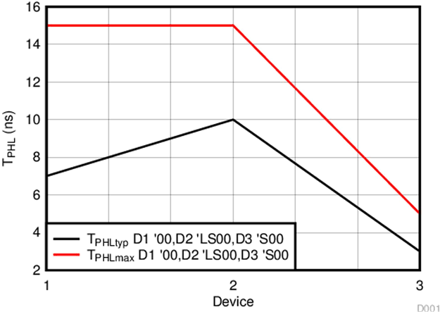
6.11 Typical Characteristics
CL = 15 pF
 Figure 1. TPHL (Across Devices)
 Figure 1. TPHL (Across Devices)