JAJSL63 February 2021 SN55LVCP22A-SP
PRODUCTION DATA
- 1 特長
- 2 アプリケーション
- 3 説明
- 4 Revision History
- 5 Pin Configuration and Functions
- 6 Specifications
- 7 Parameter Measurement Information
- 8 Detailed Description
- 9 Application and Implementation
- 10Power Supply Recommendations
- 11Layout
- 12Device and Documentation Support
- 13Mechanical, Packaging, and Orderable Information
5 Pin Configuration and Functions
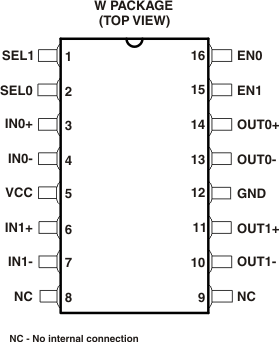
Table 5-1 Pin Functions
| TERMINAL | I/O | DESCRIPTION | |
|---|---|---|---|
| NAME | NO. | ||
| SEL1 | 1 | Input | Switch Selection Control 1 |
| SEL0 | 2 | Input | Switch Selection Control 2 |
| IN0+ | 3 | Input | LVDS Receiver Positive Input 0 |
| IN0- | 4 | Input | LVDS Receiver Negative Input 0 |
| VCC | 5 | Power | 3.3V Supply Voltage |
| IN1+ | 6 | Input | LVDS Receiver Positive Input 1 |
| IN1- | 7 | Input | LVDS Receiver Negative Input 1 |
| NC | 8 | N/A | No Internal Connection |
| NC | 9 | N/A | No Internal Connection |
| OUT1- | 10 | Output | LVDS Driver Negative Output 1 |
| OUT1+ | 11 | Output | LVDS Driver Positive Output 1 |
| GND | 12 | Ground | Ground |
| OUT0- | 13 | Output | LVDS Driver Negative Output 0 |
| OUT0+ | 14 | Output | LVDS Driver Positive Output 0 |
| EN1 | 15 | Input | Output Enable for Driver 1 |
| EN0 | 16 | Input | Output Enable for Driver 0 |