JAJSF58O MARCH 2001 – April 2018 SN65HVD230 , SN65HVD231 , SN65HVD232
PRODUCTION DATA.
- 1 特長
- 2 アプリケーション
- 3 概要
- 4 改訂履歴
- 5 概要(続き)
- 6 Device Comparison Table
- 7 Pin Configuration and Functions
-
8 Specifications
- 8.1 Absolute Maximum Ratings
- 8.2 ESD Ratings
- 8.3 Recommended Operating Conditions
- 8.4 Thermal Information
- 8.5 Electrical Characteristics: Driver
- 8.6 Electrical Characteristics: Receiver
- 8.7 Switching Characteristics: Driver
- 8.8 Switching Characteristics: Receiver
- 8.9 Switching Characteristics: Device
- 8.10 Device Control-Pin Characteristics
- 8.11 Typical Characteristics
- 9 Parameter Measurement Information
- 10Detailed Description
- 11Application and Implementation
- 12Power Supply Recommendations
- 13Layout
- 14デバイスおよびドキュメントのサポート
- 15メカニカル、パッケージ、および注文情報
11.2.1.1 CAN Termination
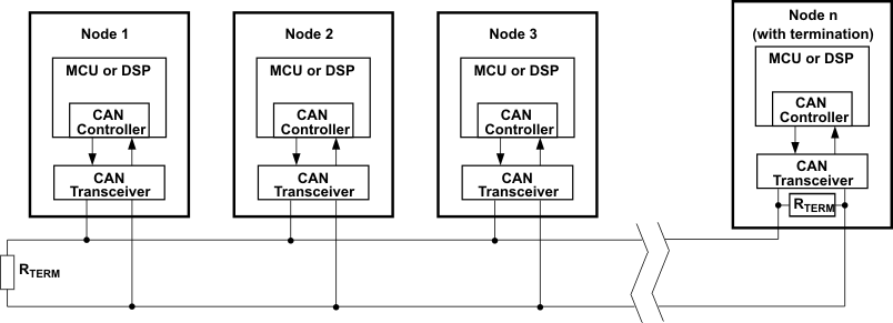
The ISO11898 standard specifies the interconnect to be a single twisted pair cable (shielded or unshielded) with 120 Ω characteristic impedance (ZO). Resistors equal to the characteristic impedance of the line should be used to terminate both ends of the cable to prevent signal reflections. Unterminated drop lines (stubs) connecting nodes to the bus should be kept as short as possible to minimize signal reflections. The termination may be on the cable or in a node, but if nodes may be removed from the bus the termination must be carefully placed so that it is not removed from the bus.
 Figure 38. Typical CAN Bus
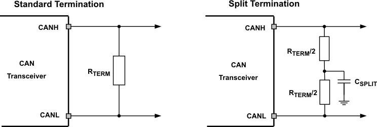
Termination is typically a 120 Ω resistor at each end of the bus. If filtering and stabilization of the common mode voltage of the bus is desired, then split termination may be used (see Figure 39). Split termination utilizes two 60Ω resistors with a capacitor in the middle of these resistors to ground. Split termination improves the electromagnetic emissions behavior of the network by eliminating fluctuations in the bus common mode voltages at the start and end of message transmissions.
Care should be taken in the power ratings of the termination resistors used. Typically the worst case condition would be if the system power supply was shorted across the termination resistance to ground. In most cases the current flow through the resistor in this condition would be much higher than the transceiver's current limit.
 Figure 39. CAN Bus Termination Concepts