JAJSPU9M september 2005 – february 2023 SN65HVD30 , SN65HVD31 , SN65HVD32 , SN65HVD33 , SN65HVD34 , SN65HVD35
PRODUCTION DATA
- 1 特長
- 2 アプリケーション
- 3 概要
- 4 Revision History
- 5 Device Comparison
- 6 Pin Configuration and Functions
-
7 Specifications
- 7.1 Absolute Maximum Ratings
- 7.2 ESD Ratings
- 7.3 Recommended Operating Conditions
- 7.4 Thermal Information
- 7.5 Electrical Characteristics: Driver
- 7.6 Electrical Characteristics: Receiver
- 7.7 Device Power Dissipation – PD
- 7.8 Supply Current Characteristics
- 7.9 Switching Characteristics: Driver
- 7.10 Switching Characteristics: Receiver
- 7.11 Dissipation Ratings
- 7.12 Typical Characteristics
- 8 Detailed Description
- 9 Application and Implementation
- 10Device and Documentation Support
- 11Mechanical, Packaging, and Orderable Information
パッケージ・オプション
メカニカル・データ(パッケージ|ピン)
- D|14
サーマルパッド・メカニカル・データ
- D|14
発注情報
Parameter Measurement Information
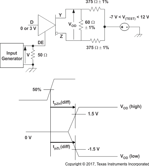
The time tpZL(x) is the measure from DE to VOD(x). VOD is valid when it is greater than 1.5 V.
Figure 8-1 Driver Enable Time From DE to VOD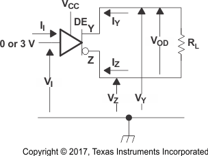 Figure 8-2 Driver VOD Test Circuit and Voltage and Current Definitions
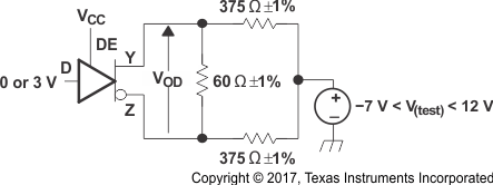 Figure 8-3 Driver VOD With Common-Mode Loading Test Circuit
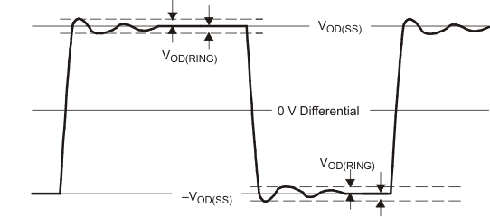 Figure 8-4 VOD(RING) Waveform and Definitions
VOD(RING) is measured at four points on the output waveform, corresponding to overshoot and undershoot from the VOD(H) and VOD(L) steady state values.
 Figure 8-5 Test Circuit and Definitions for the Driver Common-Mode Output Voltage
 Figure 8-6 Driver Switching Test Circuit and Voltage Waveforms
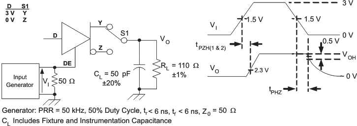 Figure 8-7 Driver High-Level Output Enable and Disable Time Test Circuit and Voltage Waveforms
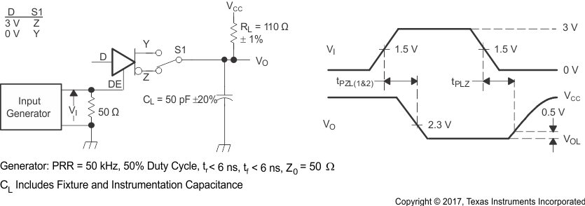 Figure 8-8 Driver Low-Level Output Enable and Disable Time Test Circuit and Voltage Waveforms
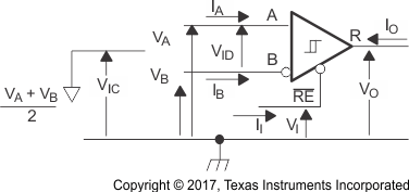 Figure 8-9 Receiver Voltage and Current Definitions
 Figure 8-10 Receiver Switching Test Circuit and Voltage Waveforms
 Figure 8-11 Receiver High-Level Enable and Disable Time Test Circuit and Voltage Waveforms
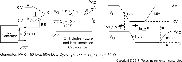 Figure 8-12 Receiver Enable Time From Standby (Driver Disabled)
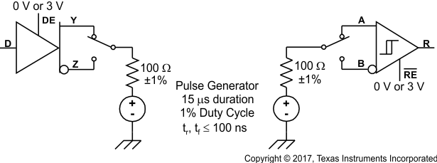 Figure 8-13 Test Circuit, Transient Over Voltage Test