JAJSQA3A june 2011 – may 2023 SN74AC14-Q1
PRODMIX
4 Pin Configuration and Functions
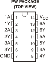
| PIN | I/O | DESCRIPTION | ||
|---|---|---|---|---|
| NAME | D, DB, N, NS, PW, J, or W | FK | ||
| 1A | 1 | 2 | Input | Channel 1, Input A |
| 1Y | 2 | 3 | Output | Channel 1, Output Y |
| 2A | 3 | 4 | Input | Channel 2, Input A |
| 2Y | 4 | 6 | Output | Channel 2, Output Y |
| 3A | 5 | 8 | Input | Channel 3, Input A |
| 3Y | 6 | 9 | Output | Channel 3, Output Y |
| GND | 7 | 10 | — | Ground |
| 4Y | 8 | 12 | Output | Channel 4, Output Y |
| 4A | 9 | 13 | Input | Channel 4, Input A |
| 5Y | 10 | 14 | Output | Channel 5, Output Y |
| 5A | 11 | 16 | Input | Channel 5, Input A |
| 6Y | 12 | 18 | Output | Channel 6, Output Y |
| 6A | 13 | 19 | Input | Channel 6, Input A |
| VCC | 14 | 20 | — | Positive Supply |
| NC | 1, 5, 7, 11, 15, 17 | — | Not internally connected | |