SCLS226K October 1995 – July 2014 SN54AHC244 , SN74AHC244
PRODUCTION DATA.
- 1 Features
- 2 Applications
- 3 Description
- 4 Simplified Schematic
- 5 Revision History
- 6 Pin Configuration and Functions
- 7 Specifications
- 8 Parameter Measurement Information
- 9 Detailed Description
- 10Application and Implementation
- 11Power Supply Recommendations
- 12Layout
- 13Device and Documentation Support
- 14Mechanical, Packaging, and Orderable Information
パッケージ・オプション
デバイスごとのパッケージ図は、PDF版データシートをご参照ください。
メカニカル・データ(パッケージ|ピン)
- DGV|20
- DB|20
- NS|20
- N|20
- DW|20
- PW|20
サーマルパッド・メカニカル・データ
- PW|20
発注情報
10 Application and Implementation
10.1 Application Information
The SNx4AHC244 is a low drive CMOS device that can be used for a multitude of bus interface type applications where output ringing is a concern. The low drive and slow edge rates will minimize overshoot and undershoot on the outputs. The inputs can except voltages to 5.5 V at any valid VCC making it ideal for down translation.
10.2 Typical Application
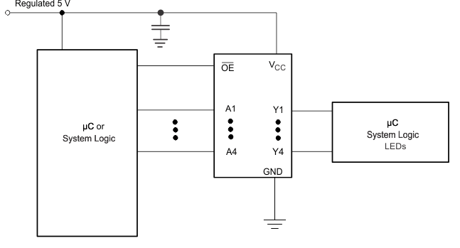 Figure 5. Typical Application Diagram
10.2.1 Design Requirements
This device uses CMOS technology and has balanced output drive. Care should be taken to avoid bus contention because it can drive currents that would exceed maximum limits. The high drive will also create fast edges into light loads so routing and load conditions should be considered to prevent ringing.
10.2.2 Detailed Design Procedure
- Recommended input conditions
- Specified high and low levels. See (VIH and VIL) in Recommended Operating Conditions.
- Inputs are overvoltage tolerant allowing them to go as high as 5.5 V at any valid VCC
- Recommend output conditions
- Load currents should not exceed 25 mA per output and 50 mA total for the part
- Outputs should not be pulled above VCC
10.2.3 Application Curves
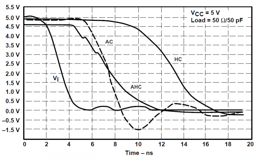 Figure 6. Switching Characteristics Comparison