JAJSP67T October   1995  – October 2023 SN54AHCT14 , SN74AHCT14

PRODUCTION DATA  

  1.   1
  2. 特長
  3. アプリケーション
  4. 概要
  5. Revision History
  6. Pin Configuration and Functions
  7. Specifications
    1. 6.1 Absolute Maximum Ratings
    2. 6.2 Handling Ratings
    3. 6.3 Recommended Operating Conditions
    4. 6.4 Thermal Information
    5. 6.5 Electrical Characteristics
    6. 6.6 Switching Characteristics
    7. 6.7 Noise Characteristics
    8. 6.8 Operating Characteristics
    9. 6.9 Typical Characteristics
  8. Parameter Measurement Information
  9. Detailed Description
    1. 8.1 Overview
    2. 8.2 Functional Block Diagram
    3. 8.3 Feature Description
    4. 8.4 Device Functional Modes
  10. Application and Implementation
    1. 9.1 Application Information
    2. 9.2 Typical Application
      1. 9.2.1 Design Requirements
      2. 9.2.2 Detailed Design Procedure
      3. 9.2.3 Application Curves
    3. 9.3 Power Supply Recommendations
    4. 9.4 Layout
      1. 9.4.1 Layout Guidelines
      2. 9.4.2 Layout Example
  11. 10Device and Documentation Support
    1. 10.1 Documentation Support
    2. 10.2 ドキュメントの更新通知を受け取る方法
    3. 10.3 サポート・リソース
    4. 10.4 Trademarks
    5. 10.5 静電気放電に関する注意事項
    6. 10.6 用語集
  12. 11Mechanical, Packaging, and Orderable Information

パッケージ・オプション

メカニカル・データ(パッケージ|ピン)
サーマルパッド・メカニカル・データ
発注情報

Pin Configuration and Functions

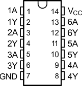
GUID-D3610BBA-E740-4533-8D09-7DCAEE1AA0CF-low.gifFigure 5-1 SN54AHCT14 J or W Package,
14-Pin CDIP or CFP
SN74AHCT14 D, DB, DGV, N, NS, or PW Package, 14-Pin SOIC, SSOP, TVSOP, PDIP, SOP, or TSSOP
(Top View)
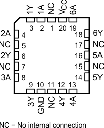
GUID-219066FE-2CD0-4CB9-A44B-6D1759CDFBF2-low.gifFigure 5-3 SN54AHCT14 FK Package, 20-Pin LCCC (Top View)
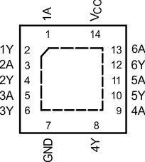
GUID-CFA4F0A6-3CFD-440E-9BEC-EA7C362DB6E7-low.gifFigure 5-2 SN74AHCT14 RGY or BQA Package, 14-Pin VQFN or WQFN (Top View)
Table 5-1 Pin Functions
PINTYPE(1)DESCRIPTION
NAMENO.
1A1I1A1
1Y2O1Y1
2A3I2A1
2Y4O2Y1
3A5I3A1
3Y6O3Y1
GND7Ground pin
4Y8O4Y1
4A9I4A1
5Y10O5Y1
5A11I5A1
6Y12O6Y1
6A13I6A1
VCC14Power pin
I = input, O = output