JAJSRC8M April 1996 – February 2024 SN74AHCT1G02
PRODUCTION DATA
- 1
- 1 特長
- 2 アプリケーション
- 3 概要
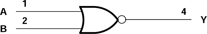
- 4 Pin Configuration and Functions
- 5 Specifications
- 6 Parameter Measurement Information
- 7 Detailed Description
- 8 Application Information Disclaimer
- 9 Device and Documentation Support
- 10Revision History
- 11Mechanical, Packaging, and Orderable Information
パッケージ・オプション
デバイスごとのパッケージ図は、PDF版データシートをご参照ください。
メカニカル・データ(パッケージ|ピン)
- DBV|5
- DCK|5