SCES592I July 2004 – September 2017 SN74AUP1G79
PRODUCTION DATA.
- 1 Features
- 2 Applications
- 3 Description
- 4 Revision History
- 5 Pin Configuration and Functions
-
6 Specifications
- 6.1 Absolute Maximum Ratings
- 6.2 ESD Ratings
- 6.3 Recommended Operating Conditions
- 6.4 Thermal Information
- 6.5 Electrical Characteristics: TA = 25°C
- 6.6 Electrical Characteristics: TA = -40°C to 85°C
- 6.7 Timing Requirements
- 6.8 Switching Characteristics: CL = 5 pF
- 6.9 Switching Characteristics: CL = 10 pF
- 6.10 Switching Characteristics: CL = 15 pF
- 6.11 Switching Characteristics: CL = 30 pF
- 6.12 Operating Characteristics
- 6.13 Typical Characteristics
- 7 Parameter Measurement Information
- 8 Detailed Description
- 9 Applications, Implementation, and Layout
- 10Power Supply Recommendations
- 11Layout
- 12Device and Documentation Support
- 13Mechanical, Packaging, and Orderable Information
パッケージ・オプション
メカニカル・データ(パッケージ|ピン)
サーマルパッド・メカニカル・データ
発注情報
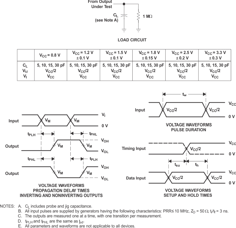
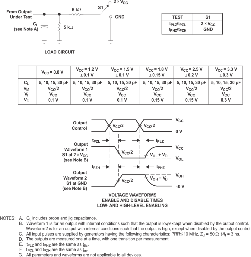
7 Parameter Measurement Information
7.1 Propagation Delays, Setup and Hold Times, and Pulse Width
 Figure 3. Load Circuit and Voltage Waveforms
7.2 Enable and Disable Times
 Figure 4. Load Circuit and Voltage Waveforms