SCDS019M May 1995 – December 2015 SN74CBT3251
PRODUCTION DATA.
- 1 Features
- 2 Applications
- 3 Description
- 4 Revision History
- 5 Pin Configuration and Functions
- 6 Specifications
- 7 Parameter Measurement Information
- 8 Detailed Description
- 9 Application and Implementation
- 10Power Supply Recommendations
- 11Layout
- 12Device and Documentation Support
- 13Mechanical, Packaging, and Orderable Information
パッケージ・オプション
デバイスごとのパッケージ図は、PDF版データシートをご参照ください。
メカニカル・データ(パッケージ|ピン)
- PW|16
- DB|16
- DBQ|16
- RGY|16
- D|16
サーマルパッド・メカニカル・データ
- RGY|16
発注情報
9 Application and Implementation
NOTE
Information in the following applications sections is not part of the TI component specification, and TI does not warrant its accuracy or completeness. TI’s customers are responsible for determining suitability of components for their purposes. Customers should validate and test their design implementation to confirm system functionality.
9.1 Application Information
The SN74CBT351 device can be used for a wide variety of applications, including expanding MCU GPIOs.
9.2 Typical Application
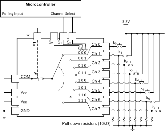
One application of the SN74CBT3251 device is to use in conjunction with a microcontroller to poll a keypad. Figure 4 shows the basic schematic for such a polling system. The microcontroller uses the channel-select pins to cycle through the different channels while reading the input to see if a user is pressing any of the keys. This is a very robust setup that allows for simultaneous key presses with very little power consumption. It also uses very few pins on the microcontroller. The down side of polling is that the microcontroller must frequently scan the keys for a press.
 Figure 4. Keypad Polling Application
9.2.1 Design Requirements
These devices use CMOS technology and have balanced output drive. Take care to avoid bus contention because it can drive currents that would exceed maximum limits.
9.2.2 Detailed Design Procedure
- Recommended input conditions:
- For switch time specifications, see propagation delay times in .
- Inputs must not be pulled below ground.
- For input voltage level specifications for control inputs, see VIH and VIL in .
- Input and output current consideration:
- Load currents must not exceed per output and must not exceed (Continuous current through VCC or GND) total current for the part. These limits are located in .
9.2.3 Application Curve
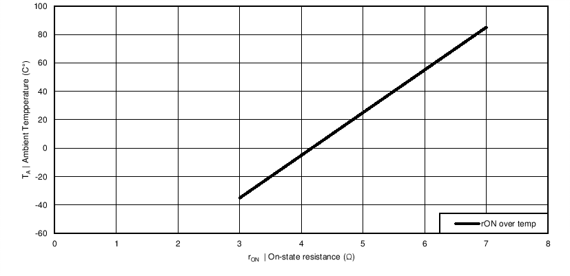
 Figure 5. rON Over Temperature