JAJSNY1F January   1996  – June 2022 SN54HC175 , SN74HC175

PRODUCTION DATA  

  1. 特長
  2. アプリケーション
  3. 概要
  4. Revision History
  5. Pin Configuration and Functions
  6. Specifications
    1. 6.1 Absolute Maximum Ratings
    2. 6.2 Recommended Operating Conditions (1)
    3. 6.3 Thermal Information
    4. 6.4 Electrical Characteristics
    5. 6.5 Timing Requirements
    6. 6.6 Switching Characteristics
    7. 6.7 Operating Characteristics
  7. Parameter Measurement Information
  8. Detailed Description
    1. 8.1 Overview
    2. 8.2 Functional Block Diagram
    3. 8.3 Device Functional Modes
  9. Power Supply Recommendations
  10. 10Layout
    1. 10.1 Layout Guidelines
  11. 11Device and Documentation Support
    1. 11.1 Receiving Notification of Documentation Updates
    2. 11.2 サポート・リソース
    3. 11.3 Trademarks
    4. 11.4 Electrostatic Discharge Caution
    5. 11.5 Glossary
  12. 12Mechanical, Packaging, and Orderable Information

パッケージ・オプション

デバイスごとのパッケージ図は、PDF版データシートをご参照ください。

メカニカル・データ(パッケージ|ピン)
  • PW|16
  • DB|16
  • NS|16
  • N|16
  • D|16
サーマルパッド・メカニカル・データ
発注情報

Functional Block Diagram

GUID-185FB6B9-D8EB-4169-A391-CCFBDC74239E-low.gif

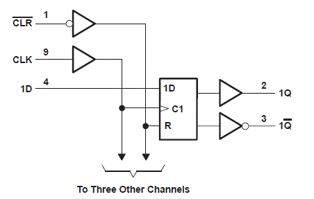
Pin numbers shown are for the D, DB, J, N, NS, PW, and W packages.