JAJSMD1F December 1982 – June 2021 SN54HC74 , SN74HC74
PRODUCTION DATA
- 1 特長
- 2 アプリケーション
- 3 概要
- 4 Revision History
- 5 Pin Configuration and Functions
-
6 Specifications
- 6.1 Absolute Maximum Ratings
- 6.2 ESD Ratings
- 6.3 Recommended Operating Conditions
- 6.4 Thermal Information
- 6.5 Electrical Characteristics - 74
- 6.6 Electrical Characteristics - 54
- 6.7 Timing Requirements - 74
- 6.8 Timing Requirements - 54
- 6.9 Switching Characteristics - 74
- 6.10 Switching Characteristics - 54
- 6.11 Operating Characteristics
- 6.12 Typical Characteristics
- 7 Parameter Measurement Information
- 8 Detailed Description
- 9 Application and Implementation
- 10Power Supply Recommendations
- 11Layout
- 12Device and Documentation Support
- 13Mechanical, Packaging, and Orderable Information
パッケージ・オプション
デバイスごとのパッケージ図は、PDF版データシートをご参照ください。
メカニカル・データ(パッケージ|ピン)
- D|14
- PW|14
- DB|14
- N|14
- NS|14
サーマルパッド・メカニカル・データ
発注情報
7 Parameter Measurement Information
- Phase relationships between waveforms were chosen arbitrarily. All input pulses are supplied by generators having the following characteristics: PRR ≤ 1 MHz, ZO = 50 Ω, tt < 6 ns.
- The outputs are measured one at a time, with one input transition per measurement.

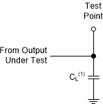
A. CL= 50 pF and
includes probe and jig capacitance.
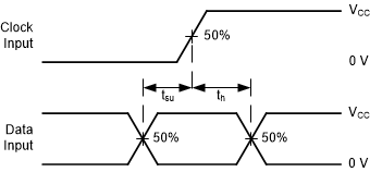
Figure 7-1 Load Circuit Figure 7-3 Voltage Waveforms
Setup and Hold Times
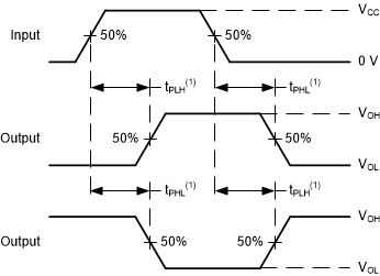
A. The maximum between
tPLH and tPHL is used for
tpd.
Figure 7-5 Voltage Waveforms
Propagation Delays
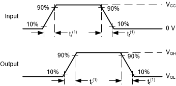
A. tt is the
greater of tr and tf.
Figure 7-2 Voltage Waveforms
Transition Times Figure 7-4 Voltage Waveforms
Pulse Width