SDLS020F May 1990 – July 2016 SN54LS06 , SN74LS06
PRODUCTION DATA.
- 1 Features
- 2 Applications
- 3 Description
- 4 Revision History
- 5 Pin Configuration and Functions
- 6 Specifications
- 7 Parameter Measurement Information
- 8 Detailed Description
- 9 Application and Implementation
- 10Power Supply Recommendations
- 11Layout
- 12Device and Documentation Support
- 13Mechanical, Packaging, and Orderable Information
パッケージ・オプション
メカニカル・データ(パッケージ|ピン)
サーマルパッド・メカニカル・データ
発注情報
9 Application and Implementation
NOTE
Information in the following applications sections is not part of the TI component specification, and TI does not warrant its accuracy or completeness. TI’s customers are responsible for determining suitability of components for their purposes. Customers should validate and test their design implementation to confirm system functionality.
9.1 Application Information
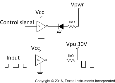
The open-collector device is suitable for high-drive and high-voltage translation applications.
9.2 Typical Application
 Figure 3. Application Schematic
9.2.1 Design Requirements
The SNx4LS06 are open-collector devices which can sink current (up to 40 mA on SN74LS06). The devices can be used in applications such as LED drivers and voltage translation using pullup resistors.
9.2.2 Detailed Design Procedure
- Recommended input conditions:
- Specified high and low levels. See (VIH and VIL) in the Recommended Operating Conditions.
- Inputs are overvoltage tolerant allowing them to go as high as 5.5 V at any valid VCC.
- Recommended output conditions:
- Load currents must not exceed (IO max) per output.
- Outputs can be pulled up to 30 V.
9.2.3 Application Curve
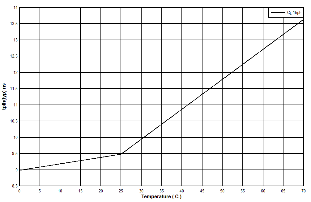
 Figure 4. Propagation Delay vs Temperature