SCLS467F FEBRUARY 2003 – June 2016 SN74LV123A-Q1
PRODUCTION DATA.
- 1 Features
- 2 Applications
- 3 Description
- 4 Revision History
- 5 Pin Configuration and Functions
-
6 Specifications
- 6.1 Absolute Maximum Ratings
- 6.2 ESD Ratings
- 6.3 Recommended Operating Conditions
- 6.4 Thermal Information
- 6.5 Electrical Characteristics
- 6.6 Timing Requirements — VCC = 3.3 V ± 0.3 V
- 6.7 Timing Requirements — VCC = 5 V ± 0.5 V
- 6.8 Switching Characteristics — VCC = 3.3 V ± 0.3 V
- 6.9 Switching Characteristics — VCC = 5 V ± 0.5 V
- 6.10 Operating Characteristics
- 6.11 Typical Characteristics
- 7 Parameter Measurement Information
- 8 Detailed Description
- 9 Application and Implementation
- 10Power Supply Recommendations
- 11Layout
- 12Device and Documentation Support
- 13Mechanical, Packaging, and Orderable Information
パッケージ・オプション
デバイスごとのパッケージ図は、PDF版データシートをご参照ください。
メカニカル・データ(パッケージ|ピン)
- PW|16
サーマルパッド・メカニカル・データ
発注情報
11 Layout
11.1 Layout Guidelines
Inputs must never float when using multiple bit logic devices. In many cases, functions or parts of functions of digital logic devices are unused. For example, when only two inputs of a triple-input AND gate are used or only three of the four buffer gates are used. Such input pins must not be left unconnected because the undefined voltages at the outside connections result in undefined operational states. All unused inputs of digital logic devices must be connected to a high or low bias to prevent them from floating. The logic level that must be applied to any particular unused input depends on the function of the device. Generally they will be tied to GND or VCC whichever makes more sense or is more convenient. Floating outputs is generally acceptable, unless the part is a transceiver.
11.2 Layout Example
 Figure 19. Layout Recommendation
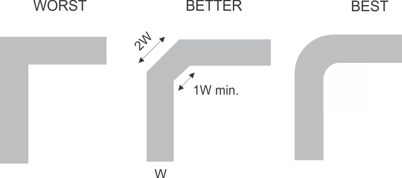
 Figure 20. Trace Example