JAJSQQ9B may 2005 – july 2023 SN74LV125AT
PRODUCTION DATA
- 1
- 1特長
- 2概要
- 3Revision History
- 4Pin Configuration and Functions
- 5Specifications
- 6Parameter Measurement Information
- 7Detailed Description
- 8Device and Documentation Support
- 9Mechanical, Packaging, and Orderable Information
パッケージ・オプション
メカニカル・データ(パッケージ|ピン)
サーマルパッド・メカニカル・データ
発注情報
4 Pin Configuration and Functions
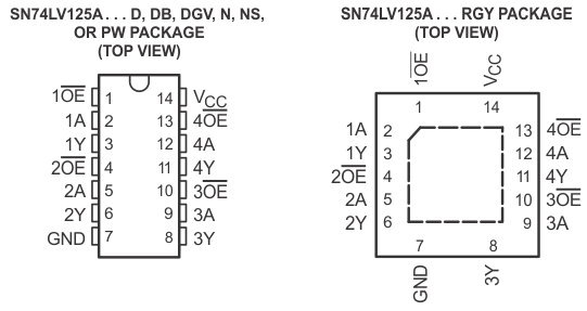
| PIN | TYPE(1) | DESCRIPTION | |
|---|---|---|---|
| NO. | NAME | ||
| 1 | 1OE | I | Output Enable 1, Active Low |
| 2 | 1A | I | 1A Input |
| 3 | 1Y | O | 1Y Output |
| 4 | 2OE | I | Output Enable 2, Active Low |
| 5 | 2A | I | 2A Input |
| 6 | 2Y | O | 2Y Output |
| 7 | GND | — | Ground Pin |
| 8 | 3Y | O | 3Y Output |
| 9 | 3A | I | 3A Input |
| 10 | 3OE | I | Output Enable 3, Active Low |
| 11 | 4Y | O | 4Y Output |
| 12 | 4A | I | 4A Input |
| 13 | 4OE | I | Output Enable 4, Active Low |
| 14 | VCC | — | Power Pin |
(1) Signal Types: I = Input, O =
Output, I/O = Input or Output.